|
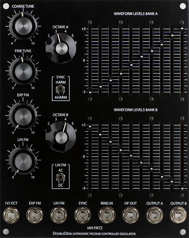
Ian Fritz DoubleDeka VCO |
|
I finally got around to building an Ian Fritz DoubleDeka VCO and bought the Bridechamber complete kit. There is a Electro-Music The DoubleDeka Ultrasonic VCO topic for this module. I changed the chicken head pointers to Moog-style knobs and the round to flatten style switches.
I used square pins with FCI housings for the interconnect wiring.
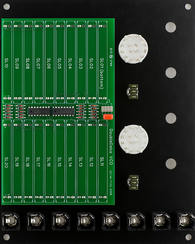
I changed the potentiometers to 1/2" square style so the bushings would fit the panel better. I had to bend the outer two pins to fit the PCB pattern. I made a custom bracket out of 0.050" aluminum to mount the PCB to the panel firmly. I used square pins with FCI housings for all interconnect wiring
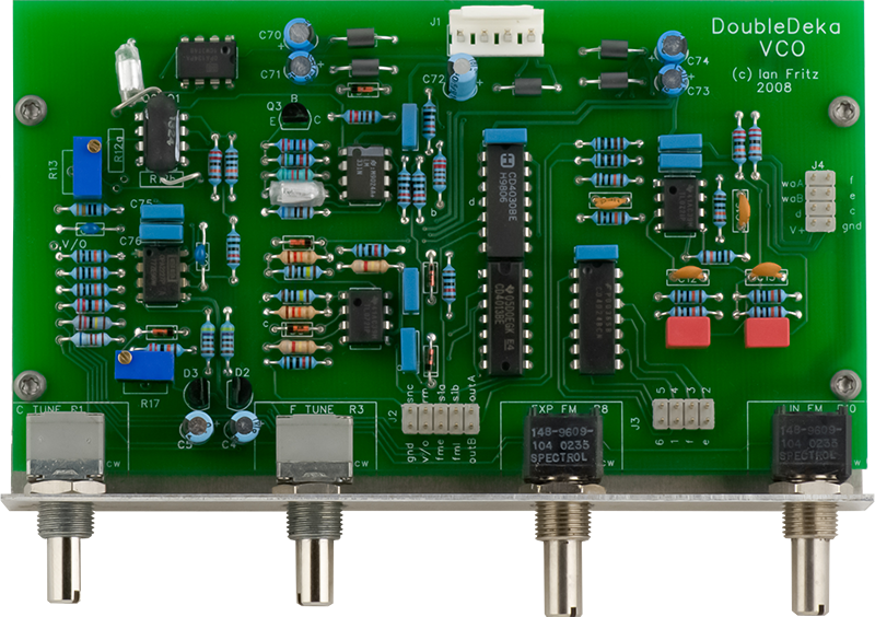
The FCI pins and housing made wiring quite easy. I used some hot glue on the connectors to make sure they stay tight. I originally wired the octave switches backwards. I had assumed the numbers on the PCB connector corresponded to the numbers on the octave switch but they do not. Wire it in reverse. The numbers must refer to the divider chain sequence so 6 on the PCB is the lowest octave and would correspond with the octave switch 1 position. This image shows a different HF Out mod which I later replaced with a comparator circuit.
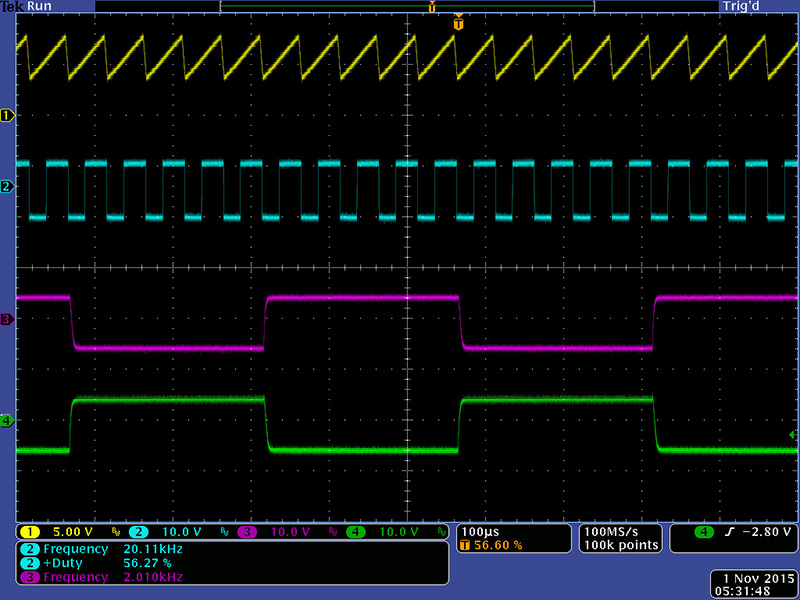
This panel has a HF Out jack for the high frequency oscillator. The output of the LM331 is a narrow pulse so I used the ramp output of A1 to drive a comparator with the threshold at 4.4V. It generates a very nice +/-5V output up to nearly the highest frequencies where it deteriorates. I put the LM311 comparator on top of U3. The output is the connection on the two resistors tied together on the left.
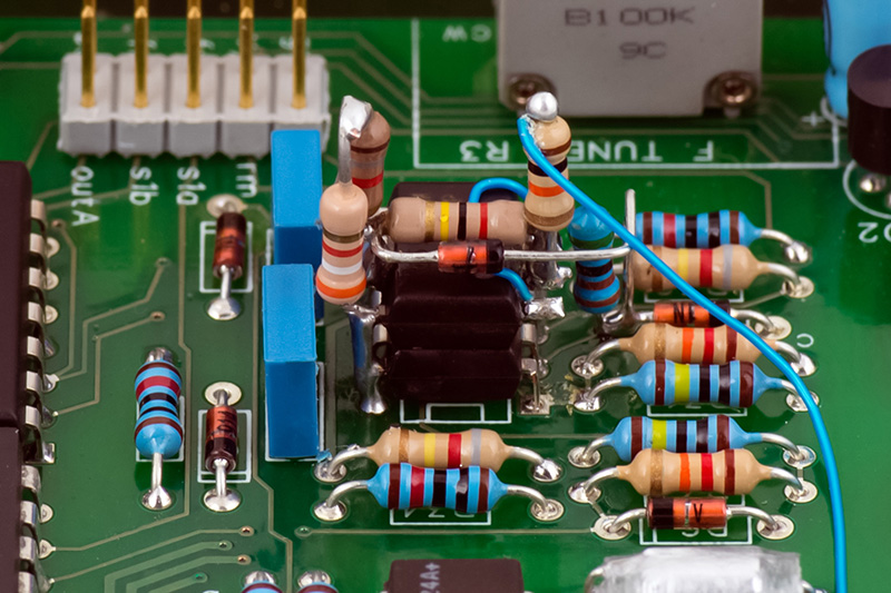
DoubleDeka HF Out modification
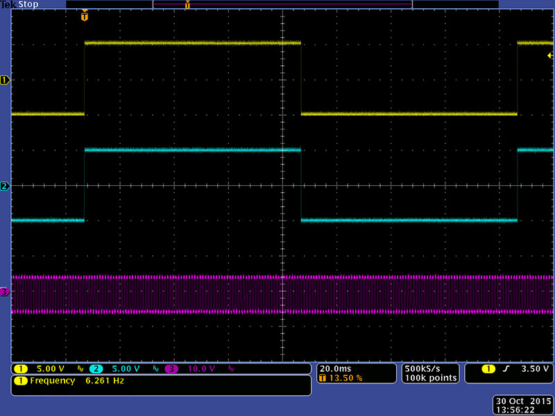
Operation
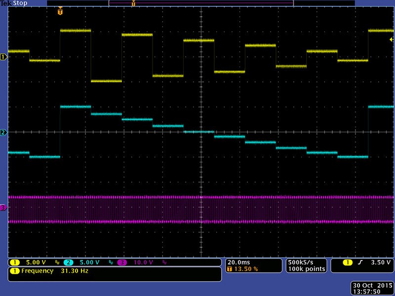
I am running this module unmodified on +/-15 power supplies. The signal level is the output level of the CD4017 decade counter attenuated by 2 and then followed by an op-amp driver with a gain of 2. The signal has a 0.7V diode drop which is compensated for by the AC coupling resulting in an output level of +/-7.5V.
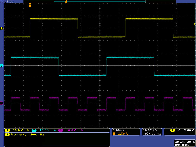
At low frequencies the tilt of the output is readily apparent due to the AC coupling. You can also see that at power up there is a random phase shift between the two banks since the two CD4017s power up at different states.
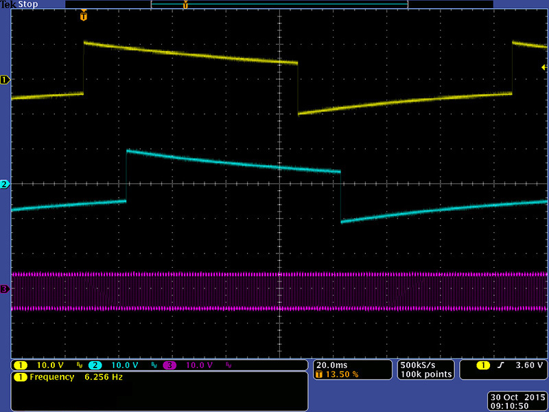
Applying a Sync or RM input synchronizes the bank outputs.
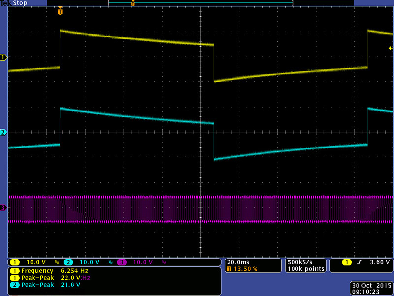
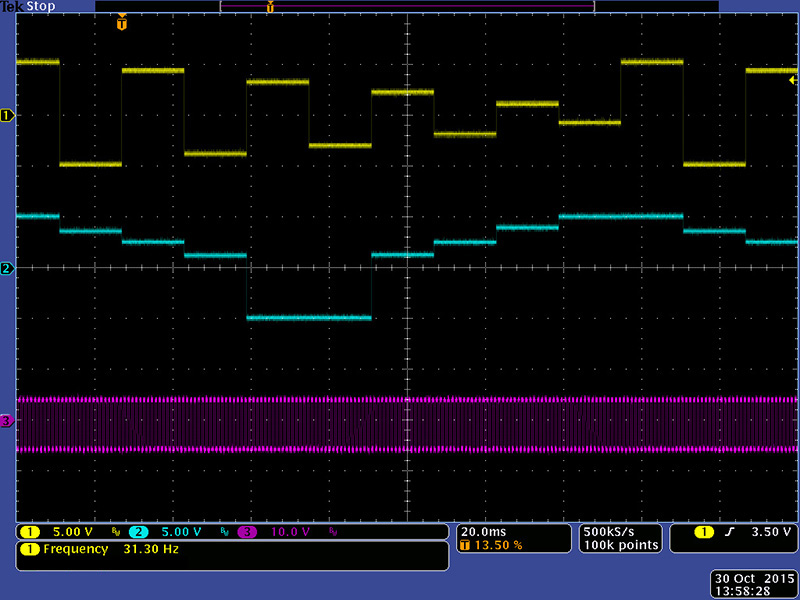
I wanted to eliminate the low frequency tilt and have the outputs be 10V pk-pk. I replaced C11 and C14 with links, changed R43 and R49 from 100K to 6K8, and added 22K resistors from U9 pin 2 to +15V and U9 pin 6 to +15V. This reduces the gain to 10V pk-pk and offsets the waveforms symmetrically around ground as can be seen in this scope image.
The yellow waveform is the ramp output of A1. Cyan is my HF Out signal which is a nice +/-5V square wave up to 10KHz.
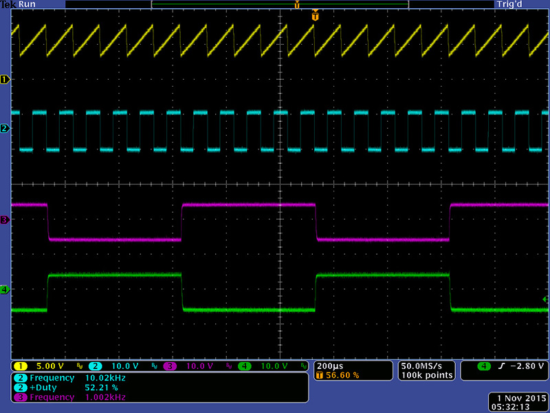
At 20 KHz the duty cycle of the HF Out begins to shift a bit.
By 40 KHz the duty cycle of the HF Out has shifted to 65% but still is a very usable signal.

Here are a couple of different waveforms drawn by the sliders.