 |
Magic Smoke Electronics |
|
I built the Thomas Henry TH-101 VCO as discussed on the Electro-Music forum. I used the Magic Smoke Electronics rev1 PCB and a 1992 date code National Semiconductor metal can LM566CH.
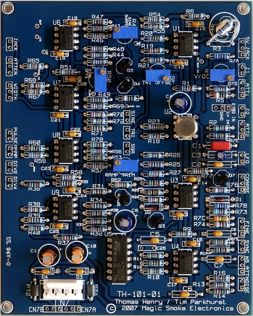
There are several minor details to be aware of:
1. A jumper is required between Tri and PWM on the PCB.
2. C4 is installed opposite of the silkscreen layout (+
towards J2)
3. Q6 is rotated from the silkscreen layout (~90
degrees CCW with 'flat' towards D2)
4. VCO stops oscillating at CCW rotation of COARSE
control (see modifications below)
5. Significant VCO crosstalk in the noise output
(see modifications below)
I created my own Mouser parts list from the schematics with minor changes in the build configuration. I chose ceramic for all the axial-style capacitors except the two timing capacitors which are polypropylene and non-polarized electrolytic. These capacitors were available in radial so the leads need to be bent to fit the PCB. I cannot guarantee that the parts list is error free so use it at your own risk.
566 VCO parts list Updated
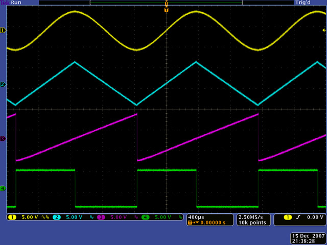
Four of the output waveforms are shown in this oscilloscope image. Initial testing indicates the oscillator is quite stable. The waveforms begin to degrade at the extreme either end of the CV range but are well behaved when operated in the center of the range.
Performance
Tracking
The oscillator is quite stable, symmetrical, and tracks well over ~4 volt range. At the
lower end of the control voltage the triangle and square waves skew from a 50%
duty cycle the
triangle linearity degrades although the the VCO is still very usable. At the higher end
of the control voltage the oscillator
begins to track flat.
Range
The VCO stops oscillating at the low end of the COARSE control. I added a
30K resistor in series with pin 3 (-15V) to potentiometer CNR1 to limit the low
end range. I do not know if the NE566 would operate differently at this
low control voltage.
The LFO frequency wasn't low enough for what I wanted. I replaced C3 with a 4.7 uF non-polarized capacitor which provides a LFO frequency range of 0.02 Hz to 120 Hz.
Ramp
The ramp waveform adjusts to be very linear. This adjustment is dependent on the triangle
offset so make sure it is adjusted first. At frequencies above 2 KHz there is a
slight notch as the phase of the square wave begins to switch the polarity of
the triangle a bit
late. This notch becomes pronounced above 6 KHz although I cannot detect any
audible artifacts. I do not know if the NE566 would have different
characteristics.
Sine
The sine wave adjusts very nicely as can be seen in the above scope image.
This adjustment is dependent on the triangle offset so make sure it is adjusted first.
Noise
The noise output has significant crosstalk from the VCO but works for FM modulation
of the oscillator. I
did some experimentation and determined that the noise was coming from the -15
volt supply to U4 and Q3. I isolated the -15 volts to eliminate the noise,
but someone pointed out later that only the base is connected to -15
volts. Changing the base to connect to ground instead of -15 volts
eliminates the crosstalk completely.
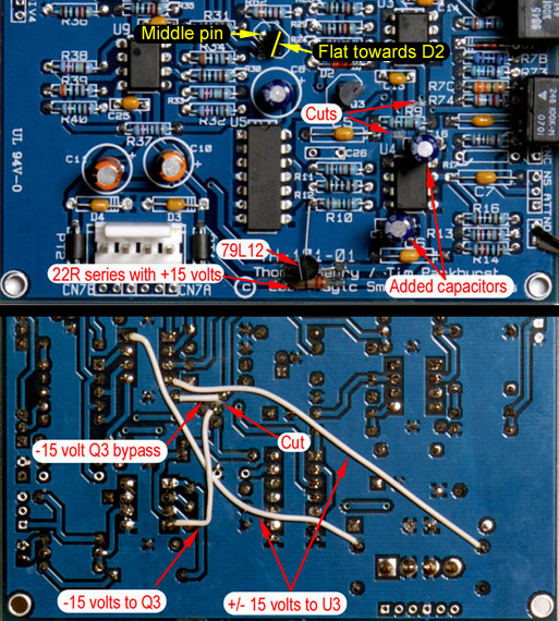
My modifications on this prototype consisted of cutting the power trace above U4 and bypassing -15 volts to U3. I had to also cut the trace to bypass the base of Q3 and wire -15 volts from U4. I cut the -15 volt trace to U4 at the bottom of the PCB and added a 79L12 regulator with a 4.7 uF capacitor across C17. I also isolated the +15 volt supply in a similar manner but used a 22R resistor and 4.7 uF capacitor across C16. The +15 volts does not contribute to the crosstalk so you can leave this unmodified. Below is a photo of my PCB modifications showing the -15 and +15 volt isolation and the orientation of Q6. I should have simply gone back to the schematic and studied how to eliminate the dependency on the -15 volts.
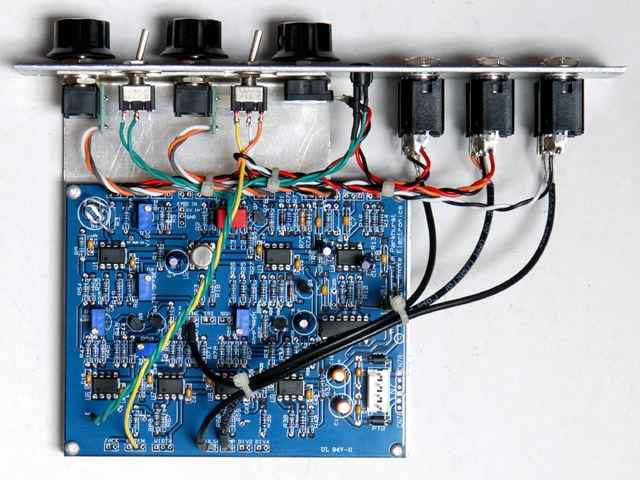
I made a mounting bracket and a 1U front panel using stock aluminum. I covered the front panel with a laser print from FrontPanelExpress and sprayed it with clearcoat. It came out pretty good as can be seen in the lower right photo although the white legends and graphics are a bit light. Perhaps increasing the line width to 0.4 mm for laser printing would better match other module panels.
Panel Design
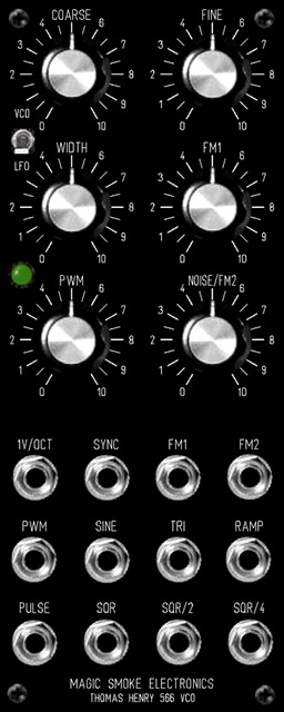
This PCB supports a total of 13 jacks, 7 potentiometers, and 1 switch. I eliminated the NOISE control and output and normalled the noise output to the FM2 input jack to fit a 2U panel as shown on the left
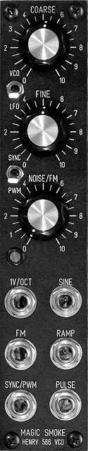
I built a prototype module as a 1U Mini-VCO / Super-LFO module as shown on the right. The upper switch selects VCO or LFO range and the lower switch selects the input between SYNC or PWM. Pulse width defaults to 50% when the control is set to SYNC. NOISE is normalled to the FM input jack and a bi-color LED indicates the frequency. Note the image on the right is an actual photograph of a panel made by gluing a laser print of the FPE design to an aluminum panel and lightly coating with lacquer.
1U VCO/LFO FrontPanelExpress design file
2U VCO/LFO FrontPanelExpress design file