 |
DJB-Echo/Delay Module |
|
STATUS: I will leave this page as a reference for a design using the CGS-44 PT2395 Delay. |
|
|
||||
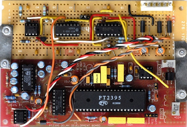
I built this module around the CGS-44 PT2395 Delay Development board and designed additional support circuitry for CV controlled delay and bypass, gain and loopback controls for echo, and an output mix control. This architecture is very similar to my DJB-012 Tape Interface
I like the short setting best although overall performance doesn't degrade much with either the medium or long delay settings. The output level of the PT2395 is attenuated when either medium or long is selected so I added a jumper to increase the output gain for these settings.
The delay CV circuit uses a varactol to adjust the RC oscillator in the PT2395. The first stage of this circuit is a sum and rectifier to add and limit the control voltage to negative values (inverted signal). The second stage is a "greater than" circuit to select the greater of either the summed control voltage or -5 volts. This limits the control voltage to between 0 and -5 volts no matter what the delay input and control are set to. Two adjustment trimmers limit the varactol resistance to between 1K and 6K ohms.
I tried to use the PT2395 reset pin to implement the bypass. It almost worked but here is a slight gap in the resulting audio as the PT2395 restarts so I used a HI-303 analog switch to bypass the output. The control voltage for the analog switch is a buffer wired-OR of the bypass input and switch. A jumper selects whether this bypass affects delay and echo or just echo.
Power requirements for this module is +5 volts at 22 mA, +15 volts at 35 mA, and -15 volts at 18 mA.
CGS-44 Delay Development Board schematic modifications (schematic used with permission by Ken Stone)
I cut off the CGS-44 Delay Development board to fit a Stooge bracket along side a prototype board for the additional circuitry. I mounted the varactol and the two adjustment trimmers in the empty area of the CGS-44 board to be close to the PT2395. I also modified the gains of the input and output buffers to minimize clipping. The speed jumper disconnects the varactol from the PT2395 for adjusting the minimum and maximum resistance and another jumper selects short, medium or long delay settings.
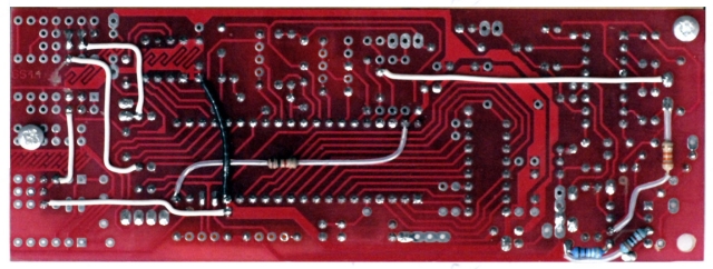
This photo shows the rear of the CGS-44 Delay Development board with the modifications for the input and output buffers, varactol, and adjustment trimmers. The black wire is a digital ground which was cut when the board was shortened.
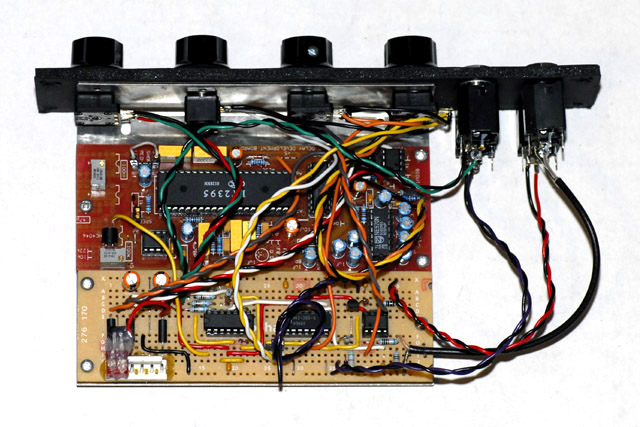
This is a photo of a completed prototype built with a foam-core prototype panel. The lower looped wire is for the bypass switch which is not installed. I added a 7805 regulator on a 2 pin MTA housing so I could operate this module from a 4 pin MOTM +/15 volt system.
This is my FrontPanelExpress panel design.
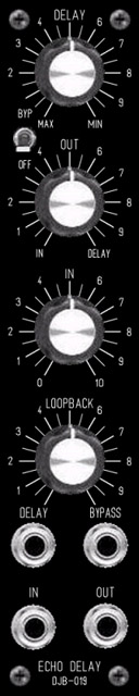
DJB-Echo/Delay FrontPanelExpress design file