|
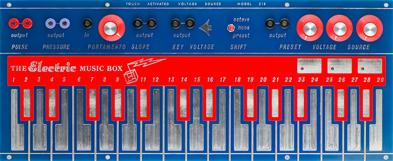
218 Touch
Activated |
|
V1
I built a 218 V1 Touch Activated Voltage Source module for myself to go with my 208 Stored Program .
Construction
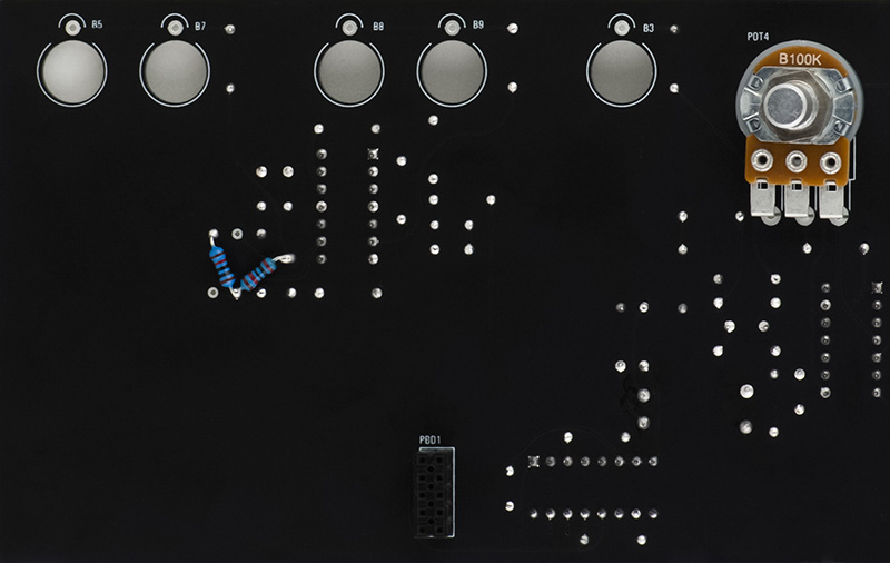
My two PCBs were pre-coated with clear and pre-soldered together. There was masking tape over the un-stuffed SMT pads and removing the tape stripped the clear coat which has no impact but looks sloppy. I cleaned the frets up by filing the ends flat and removing the red paint. Paint doesn't adhere very well to the nickel plated frets and I think the bright nickel finish looks fine. I glued the frets on with epoxy and made sure it was flush around the bottom edge for 1/2" for mounting. I used masking tape on the top to keep any epoxy from bleeding through.
One of the preset pads and most of the red PCB keys were inoperative as they were soldered without first removing the clear coat. I simply removed the solder, used a knife to clear away the clear coat on the red PCB, and resoldered.
Programming / Calibration
I had a difficult time finding the correct software to use with the ST-Link/V2. Ignore all the documentation that comes with the ST-Link/V2. You need the STM32 ST-LINK utility STSW-LINK004. You may also need the STSW-LINK009 USB drivers for Windows 7, 8, and 10. I used firmware 218-v1.1-2.hex and programming was simple and easy. There isn't a clear indication that programming is complete so I waited until there were no more messages and then selected disconnect and powered down. I calibrated the 218 by trimming the voltage to two octaves when pressing that key pad. The scaling isn't perfect but pretty close.
Operation
Operation is pretty straightforward. A DIP switch selects the output scale, first or last note, and the amplitude of the output pulse at either 10V or 13.5V.
The octave switch has three modes. If the switch set to On you can use the Preset Voltage touch pads to jump octaves (0, 1, and 2) on the Key Voltage Out jacks and Slope CV Out jacks. If the switch is set to None then the CV generated from the Preset Voltage Source knobs is only on the Preset Voltage Output jacks. If the switch is set to Preset then the CV generated from the Preset Voltage Source knobs is added to the Key Voltage Out jacks, the Slope CV Output jacks and also to the Preset Voltage Output jacks.
Modifications
There is a 13.5V supply for the preset controls generated by an op-amp running on +/-15V. This is too close to the rails and if you turn all three Preset controls up the supply droops. I changed R1 from 6K8 to 15K to drop the Preset control to 12V maximum. This isn't the full 13.5V range but the voltages remain stable.
The Pulse output is a 10V trigger with a 5V gate. I increased this to a 15V trigger and a 7.5V gate by changing R41 from 10K to 20K.
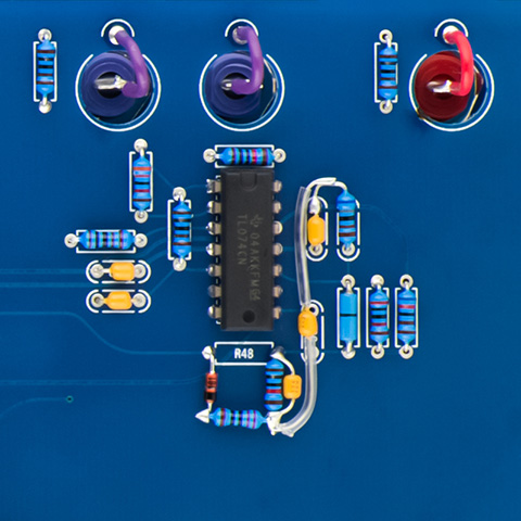
There is no offset trimmer. I added one. Connect the CCW and CW terminals of a 100K trimmer to +/-15V. Connect the wiper to a 6M8 resistor. The other side of the resistor connects to the node of R28 and R29. You can now trim the bottom key to 0.00V. Adjust this before the scale.
The Portamento control is no glide at CW and maximum glide at CCW like the original. However, the useful range is only on the 1/3 rotation from CCW. You want a log feel to portamento but this is super log. The circuit has a couple of breakpoints designed in the response curve and one uses a zener. The op-amp output is negative and the zener is backwards, and corrected is 6V which seems like too high a voltage. No portamento is when the LED is on so the issue is it doesn't go off soon enough. I played with the circuit but I always had some slew at minimum. It was getting too involved and I didn't feel like redesigning the circuit so the simple solution was to bypass some of the LED current by putting a resistor across it. I found a value between 1K and 1K5 worked best. I ended up series connecting a 1K and 270R which gave me 1.8 seconds maximum and 0.5 seconds at mid position. This circuit is the same on V2.
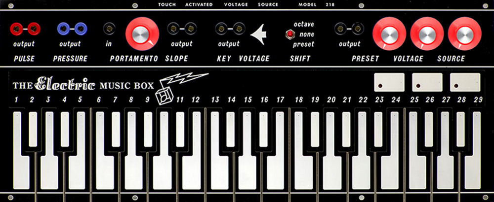
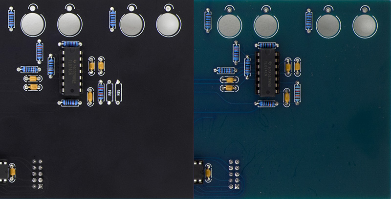
V2 Black
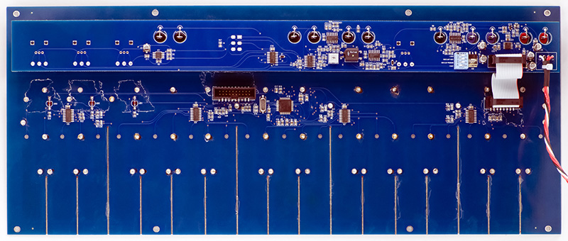
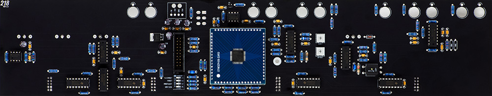
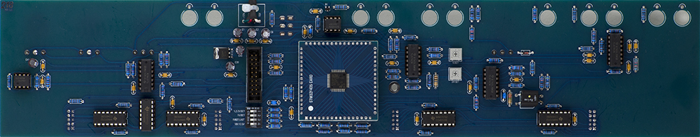
I built the black V2 for someone else. This design is similar to V1 but is mostly through-hole construction. The STM32F405 processor is on a separate daughter card and uses different firmware than V1. One main difference with the V2 design is a true two-level trigger/gate pulse output. V1 has just a single level pulse output.
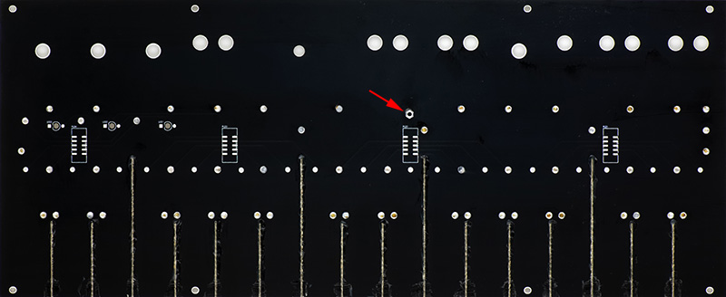
It is critical that you countersink the hole in the large PCB for a flat head 3mm screw and mount the standoff BEFORE you assemble the two PCBs. The countersunk hole and standoff is indicated by the red arrow on the back of the PCB. The standoff is not in the BOM and is a 15 mm F-F. After you mount the standoff, you align the two PCBs and solder the holes to secure them together. I did apply a little downward pressure to make sure the PCBs were flush but if you heat the bottom pad and apply solder it will wick up to the sides. I soldered all the mounting holes first and then soldered the interconnect holes for the keys.
I installed the frets with hot melt glue. I used my soldering iron at 450°F to level off the hot glue on the lower 1/2" of the PCB so the module will sit flush in a boat.
 |
The keypads are capacitive and connect directly to CMOS
inputs. You need to insulate from touch these by spraying the front of
the PCBs where the keypads are. You don't have to spray the entire
front but it is easier as there is no good mask line for just doing the
keypad area. You do not have to spray the rear of the PCBs.
I did all the soldering on PCB1 before I clear coated it so heat from soldering would not discolor the clear coat. I used tac rags to clean my bench and the PCB and and then applied Krylon Crystal Clear Acrylic Coating 1303 gloss in one coat. Even so, this acts as a dust magnet and there are a few areas with some minor dust |
 |
On other modules I used Krylon Crystal Clear Acrylic Coating K05353007 flat in multiple coats and found dust does not show. In fact it is difficult to determine that it is even clear coated. |
Unlike V1, V2 is mostly through hole construction on PCB2.
Construction is straightforward. I temporarily installed the daughter card and straight pins into the headers to align them when I soldered the headers on PCB2 and the pins on the processor daughter card.
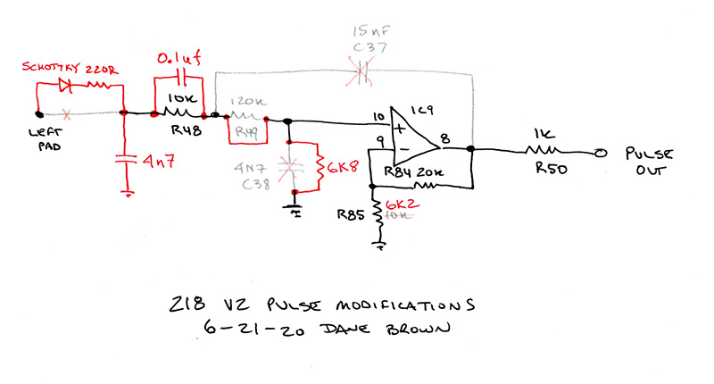
I used two of the existing resistor holes for the mod. The BOM likewise doesn't list the 10K and 20K resistors needed. On this PCB2 there was no trace between IC9 pins 8 and 9. Later I built a blue V2 PCB set which is slightly different in this area.
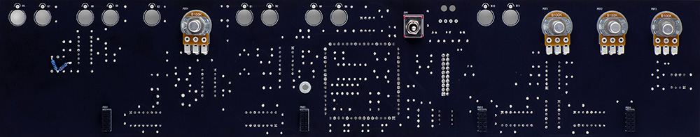
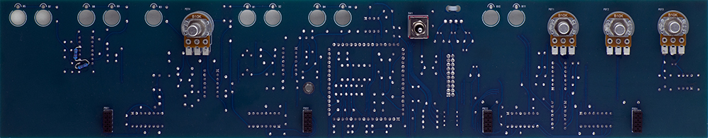
This is the finished PCB2. I have not soldered the switch and have only soldered the middle pin of the four potentiometers before assembly. Once assembled, I aligned the switch and potentiometers to the 15mm standoff and PCB to PCB connector height and then soldered them.
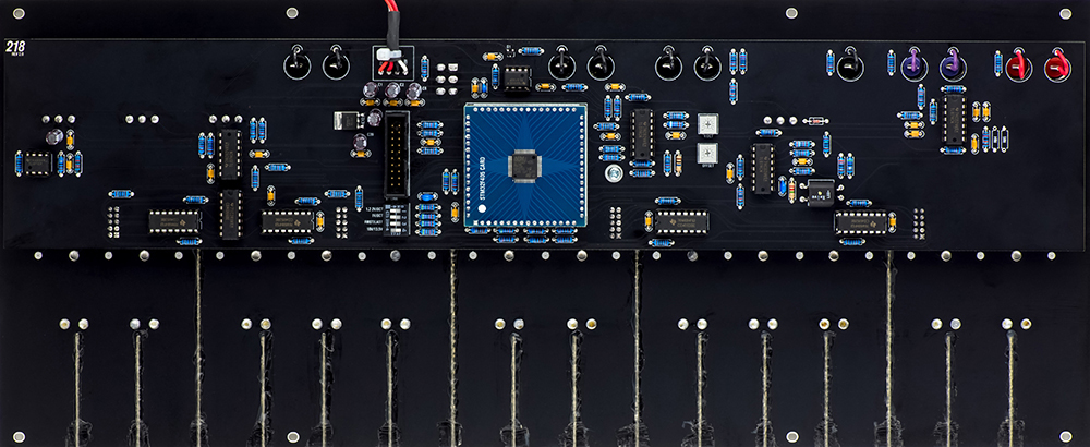
Here is the finished module.
Programming / Calibration
Programming V2 is similar to V1. You need the STM32 ST-LINK utility STSW-LINK004 and you may also need the STSW-LINK009 USB drivers for Windows 7, 8, and 10. I used firmware B218-v2.0.hex and programming was simple and easy. There isn't a clear indication that programming is complete so I waited until there were no more messages and then selected disconnect and powered down. I calibrated the 218 by trimming the voltage to two octaves when pressing that key pad.
Operation
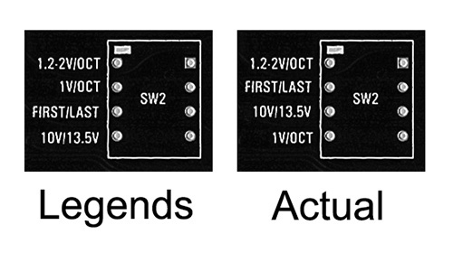
Operation is pretty straightforward. A DIP switch selects the output scale and first or last note. There is no selection for the output pulse. The legends for the DIP switch are incorrect. The third DIP switch selects either 10V or 13.5V for the pressure output.
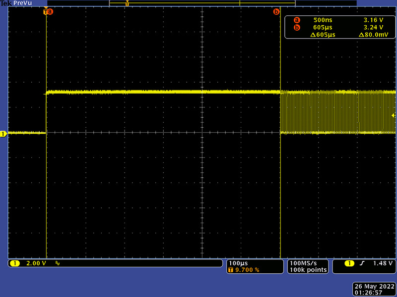
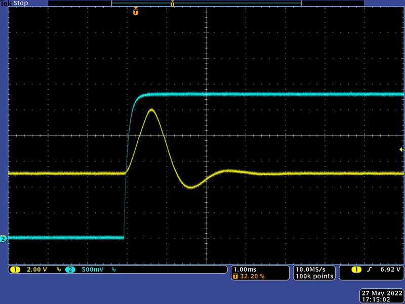
The output pulse is a combination trigger-gate pulse as seen in this scope waveform. The leading edge trigger pulse is always the same amplitude and width and the gate portion stays at 5V as long as the key is pressed. It does not have a sharp risetime and this can be an issue when triggering the 281.
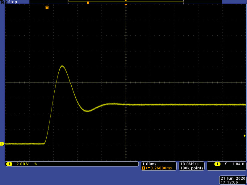
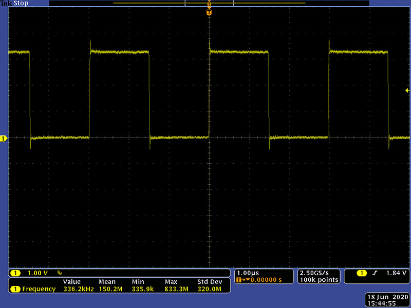
The reason for the slow rise time is the gate output from the processor is a square wave at 336 KHz so the gate circuit is a 2 pole filter with overshoot. Strange.
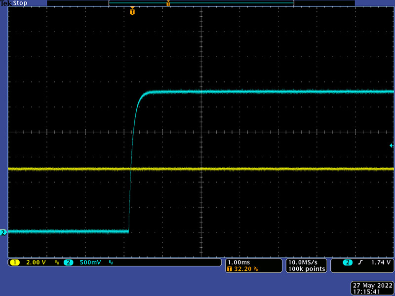
I designed this modification for a peak-detector/follower with a diode and 4n7 capacitor to convert the square wave into a gate. The 220R series resistor minimizes peak current from the microprocessor output pin. This is followed with a traditional pulse generator using a voltage attenuator with a capacitor in parallel with the top resistor. The series diode drops the smoothed gate voltage to ~ 2.9V so additional gain is required by changing the op-amp feedback resistor.
The resulting pulse output is a very traditional 10V trigger/gate which triggers the 208 and the 281.
The single black stripe resistor is a link.
Like the V1 there is a 13.5V supply for the preset controls generated by an op-amp running on +/-15V. This is too close to the rails and if you turn all three Preset controls up the supply droops. I changed R52 from 6K8 to 15K to drop the Preset control to 12V maximum. This isn't the full 13.5V range but the voltages remain stable.
V2 Blue
I later built a blue V2 PCB set.
Unlike the black V2, this PCB requires the trace on IC9 pins 8 and 9 to be cut and the two resistors added on the rear. Another major error is the power connector is screened +12V when it should be +5V. I also added a 1K5 resistor across the vactrol LED to better linearize the control.
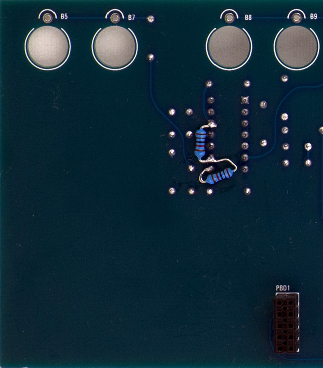
This photo shows the differences between the black and blue V2 PCBs. The black has the two resistors added, although wired wrong on this version. I suspect later revisions have been corrected.
Epilog
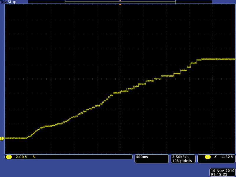
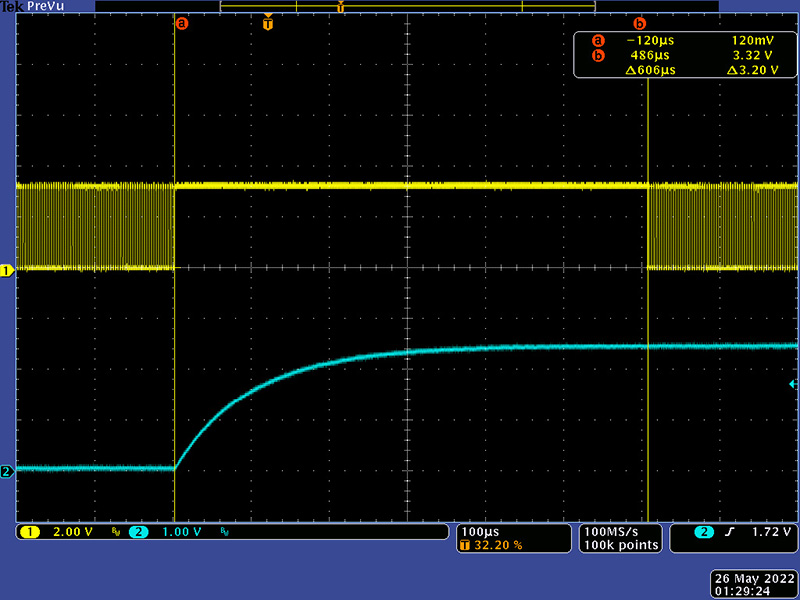
When testing out the V2 Blue module I noticed the pressure CV output exhibits steps. I hadn't noticed this before but I sometimes check pressure with a DMM. What is interesting is the steps get larger the greater the voltage. This is varying pressure set at the 10V range.
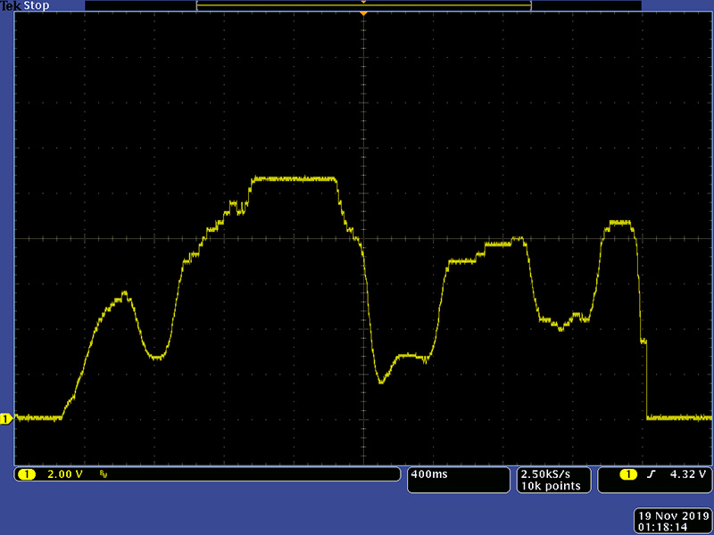
This is my attempt at a linear pressure ramp. The steps are clearly seen getting larger at the higher voltage output.
I went and checked my V1 218 and sure enough it exhibits the same issue. I patched my pressure CV to my 208 keyboard CV and they aren't that noticeable unless the pressure change is very slow. Then one can clearly hear pitch shifts in steps.
Epilog2
The stock V2 does implement a second trigger on last note priority if a second key is pressed while a first key is held ... most of the time. It does not do it on a repeat key. For example, if you hold the low note and press the high note you will get a second trigger and the new CV. When you let go of the high note, but continue to hold the low note, the CV will fall back to the original note. But if you press the same second key you will NOT get another trigger. It is for this reason I didn't worry about a second trigger on last note priority with my modification.
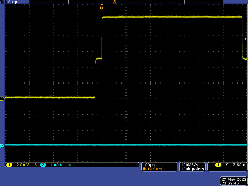
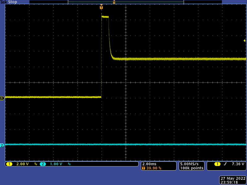
There has been some discussion on Modwiggler about this so I decided to document this further. The pulse output of the processor is a gated 336 KHz square wave. This scope image shows the signal with an initial press.
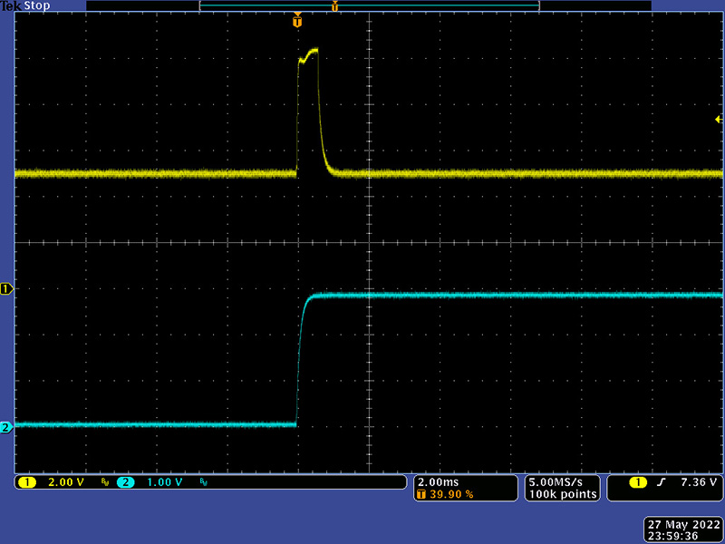
This scope image shows a second key press while holding the first.
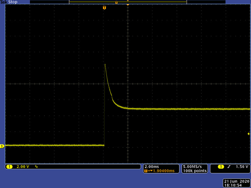
The filter produces this trigger on the second key.
There is no trigger if you release and press the same key again. You can see the CV change on the repeat key press.
This would have been so simple to implement with two processor pins and required only two resistor and the gain op-amp instead of this gated square wave and filter.
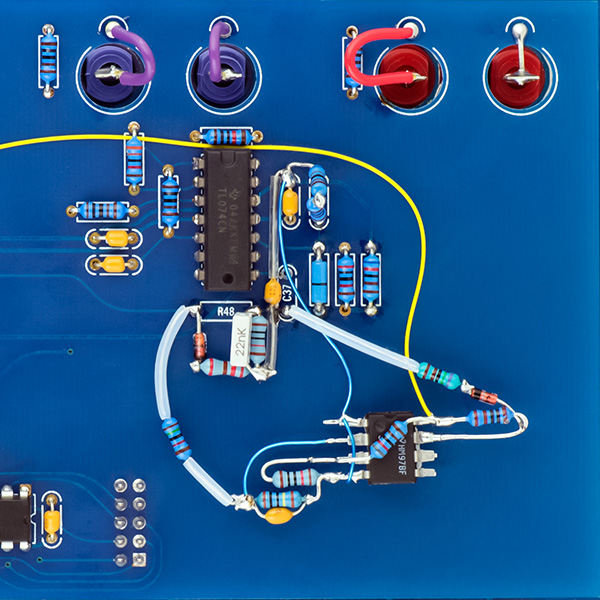
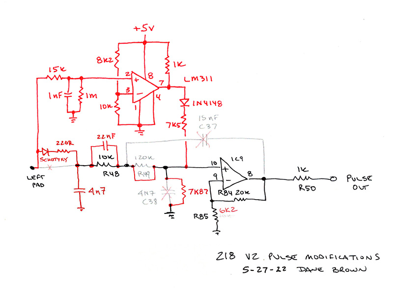
While I don't use last note priority, I decided to implement a modification to address this. I added a low pass filter to detect the gaps and a LM311 comparator to generate a trigger pulse. I add this to the original pulse modification but removed the 100 nF capacitor across R48. It works reasonably well but there is a difference in propagation time between the two circuits resulting in this extra 25 µS step on the rising edge. I don't know how this might impact the modules requiring fast rise time.
I added back a smaller 22 nF capacitor which holds the step long enough for the delay of low pass filter and comparator. This results in a good first key pressed trigger.
The trigger high portion on a second key press is a bit distorted but this shouldn't matter. I might have been able to fine tune the levels between the two circuits but decided this was good enough.
The mod isn't exactly pretty, and there might be a better solution overall, but I decided to keep the original modification mostly intact and add to it. There are two component changes on the original modification.
This would have been so simple to implement in software using two processor pins ...
The modification isn't too bad and the leaded components help hold the LM311 in place. The two resistors for C38 is because I didn't have a 7K87 value.