|
266 Source Of
Uncertainty |
|
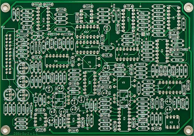
I have V1.1 of the PCB set. PCB 2 receives power from the THRU pads and I had to shift R36 and R39 slightly to allow room for a 0.1" MTA connector for a cable from PCB 1.
The noise outputs are all reasonable levels for +/-5V outputs.
The fluctuating voltage is a straightforward design and is setup for 10V CV. I made modifications for 5V CV input and 5V outputs.
The outputs of the quantized random voltages are 0 to +10 volts. The CMOS logic in this circuit operated on +10V so input protection is required from the op-amp comparators since it swings from rail to rail. The original protection circuitry consists of a series resistor/divider to limit the current and rely upon the over and under voltage protection diodes in the 4000 series CMOS. I find 4000 series CMOS fragile enough so I modified the circuit with schottky over and under voltage protection. Note that the CD4006 shift register clocks on the falling edge of the clock so no inversion is needed for the QRV Clk In. I also made modifications for 5V input and outputs.
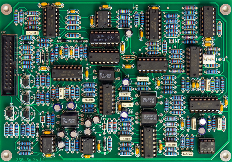
PCB 2 Modifications: (Note: applies to the 266c-5U-2 v1.1 board)
Noise
Fluctuating Random Voltages
Quantized Random Voltages
|
Noise and FRV schematic modifications
PCB 2 Mouser Excel BOM Updated
PCB 2 power consumption measurement: +15 @ 76 mA, -15V @ 58 mA (vactrol LEDs on, no output LEDs)
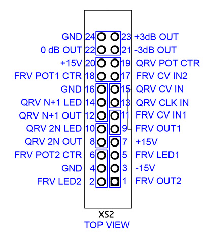
2x1, 3x1, 4x1 and 2x2 FCI mini-latch connectors fit inside the XS2 ribbon connector header to connect the front panel wiring.
Noise Operation
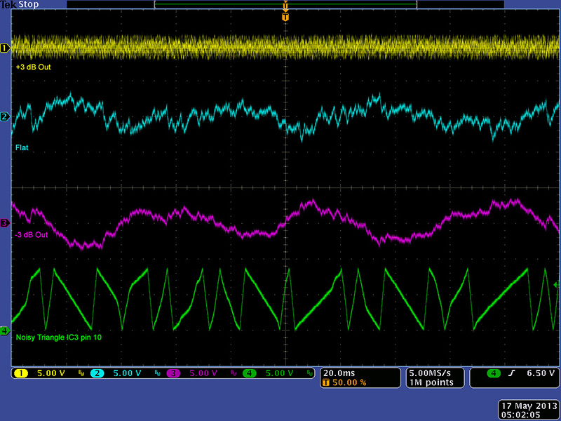
I used a vintage unlabeled MM5837 noise IC. This scope image shows the three noise outputs and the noisy triangle that is used for the FRV circuits. The noise output levels are within +/-5V levels. The MM5837 does have a short repeat length and suffers from the "chug" "chug" train sound characteristic.
I decided after using the module for a while to upgrade the noise IC to the Electric Druid noise source. This IC is a 12F675 PIC microprocessor and requires +5 volts and a resistor change for the difference in output level. I made a small adapter and sandwiched a 78L05 and a 2 µF capacitor between an 8 pin DIP header and a socket and wired up pins 1, 3 and 8 although I used pins 5 and 7 to support the socket as they are not connected on the PCB. I also change R69 from 39K to 6K8. The Electric Druid chip works great!
FRV Operation
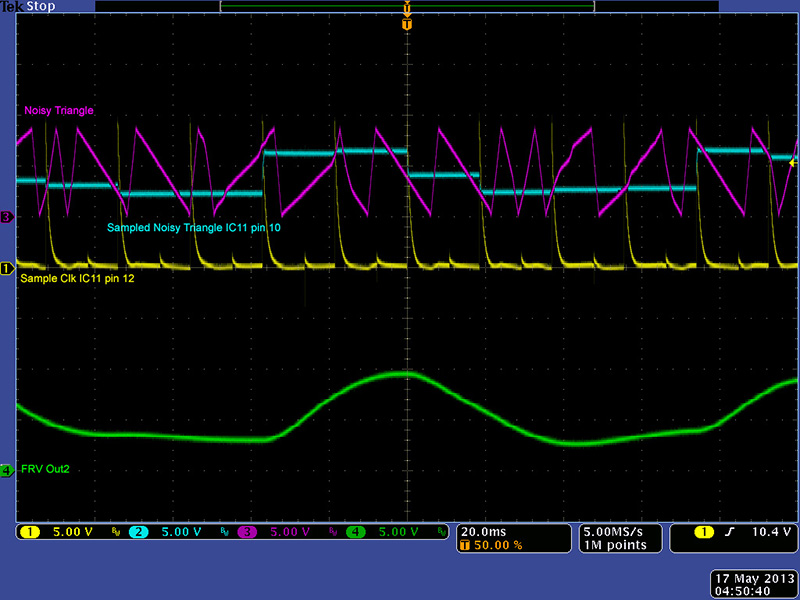
The frequency of the 556 VCO is controlled by the FRV CV. The VCO output is differentiated to form a narrow sample clock. This scope image shows the sample clock (yellow) which samples the noisy triangle (magenta) resulting in the stepped waveform (cyan) which is filtered to generate the fluctuating random voltage (green) 0 to +10V output. This circuit was the basis for the Wiard Wogglebug and the Wogglebug DIY PCB.
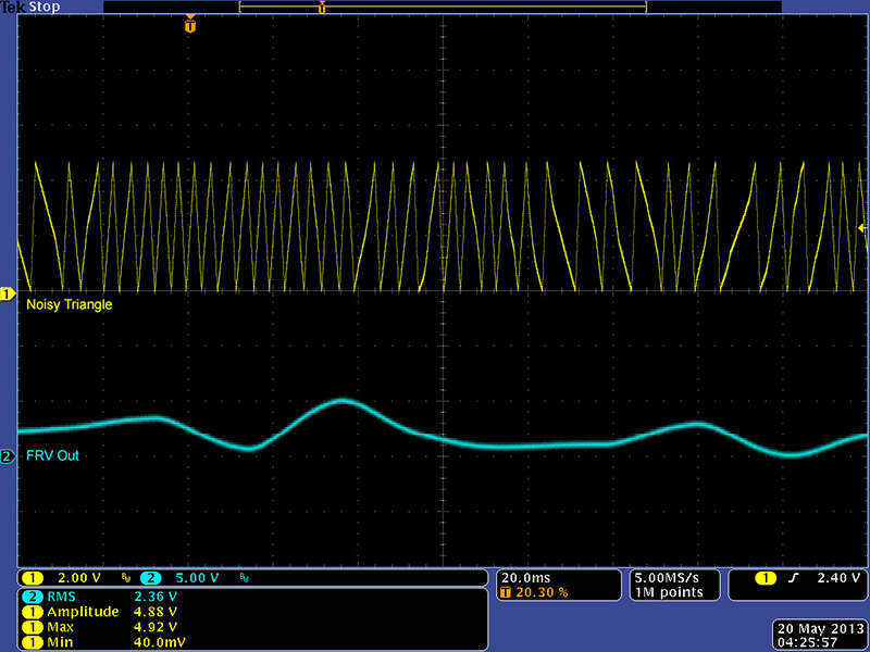
I prefer an output voltage in the range of 0 to +5 volts so I changed the noisy triangle to 0 to +5V so the FRV outputs will also be 0 to +5V as seen in this scope image.
QRV Operation
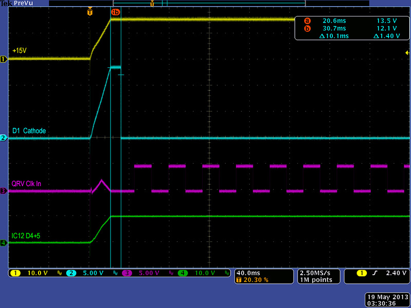
The power-on set circuit comprised of IC9A and IC10B ensures that there are logical 1's in the shift register when it is first clocked. The D1 cathode is forced high on power-on and remains high until D4+5 is at a logic 1. Note that my CD4006 happens to powers up D4+5 to a logic 1 state so this circuit doesn't really do anything. Note that the input voltage to IC12 pin 6 is +15V through a 10K resistor so I added a schottky diode to clamp this to +10V.
Both QRV outputs are quantized (e.g. discrete) voltage steps, but not to any particular V/Oct scale. Also note that the CMOS logic outputs will not drive to 0V so there is a minimum voltage offset. The QRV produces pseudo-random voltages in discrete steps but not musically scaled steps.
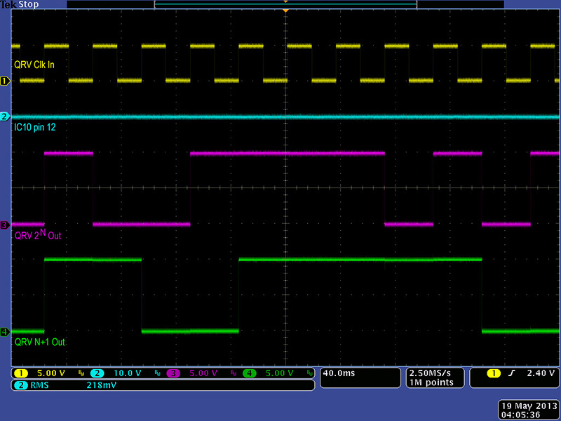
The QRV CV In and Quantization control varies the number of bits from 1 to 6 in both resistor ladders. The 2N Out is a 1 to 6 bit binary weighted resistor ladder that divides the 10V into the number of steps shown in the following table.
| No of Bits | Divider | Step Size |
| 1 | 1 | 10V |
| 2 | 3 | 3.333V |
| 3 | 7 | 1.429V |
| 4 | 15 | 667 mV |
| 5 | 31 | 323 mV |
| 6 | 63 | 159 mV |
The N+1 Out is a 1 to 6 bit linear weighted resistor ladder that divides the 10V into the number of steps shown in the following table.
| No of Bits | Divider | Step Size |
| 1 | 1 | 10V |
| 2 | 2 | 5V |
| 3 | 3 | 3.333V |
| 4 | 4 | 2.5 |
| 5 | 5 | 2V |
| 6 | 6 | 1.667V |
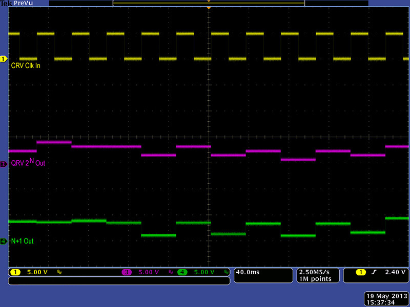
As mentioned in the SRV operation the Vol of the CMOS gate measured 371 mV and the Voh measured 10V so the actual steps are a bit smaller than in the table. In this scope image you can see the 10V steps for both 2N and N+1 outputs when the IC10 pin 12 control voltage is near 0V.
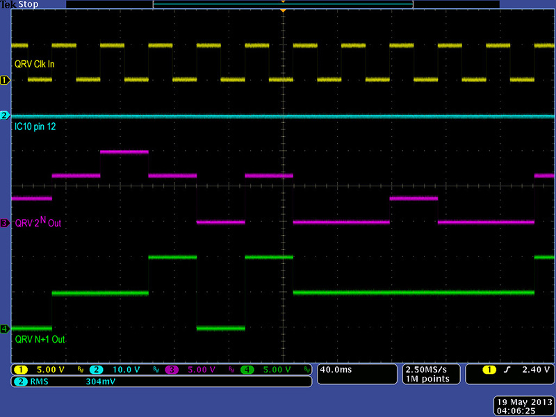
In this scope image you can see the 3.33V step for 2N output and the 5V step for N+1 output when the IC10 pin 12 control voltage is at 300 mV.
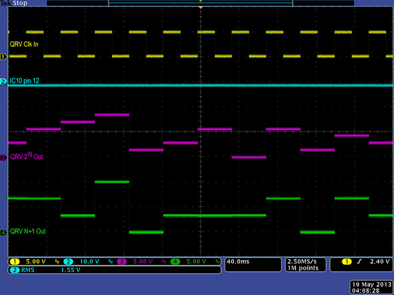
In this scope image you can see the 1.43V step for 2N output and the 3.33V step for N+1 output when the IC10 pin 12 control voltage is at 1.5V.
In this scope image you can see the 0.66V step for 2N output and the 2.5V step for N+1 output when the IC10 pin 12 control voltage is at 2.9 mV.
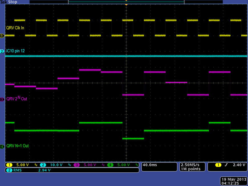
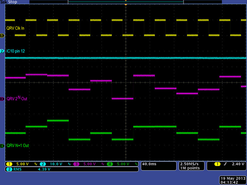
In this scope image you can see the 323mV step for 2N output and the 2.0V step for N+1 output when the IC10 pin 12 control voltage is at 4.4V.
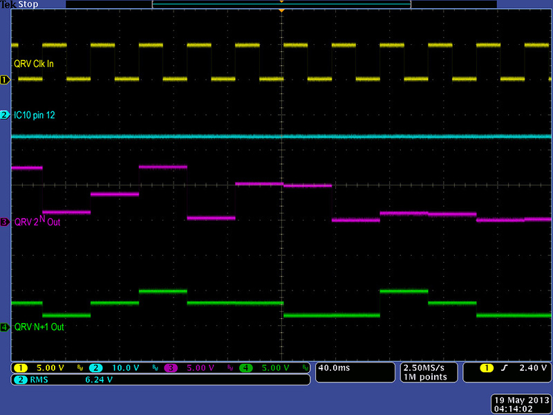
In this scope image you can see the 159mV step for 2N output and the 1.66V step for N+1 output when the IC10 pin 12 control voltage is at 6.2V.
Finally, I prefer an output voltage in the range of 0 to +5 volts. This one is easy - exchange R2 and R6 to change the +10V supply to a +5V supply. There is already over voltage protection on all the CMOS inputs so the QRV range and steps are half as shown in this scope photo.
|
|
|||||||||||||||||||||||||||||||||||||||||||||||||