 |
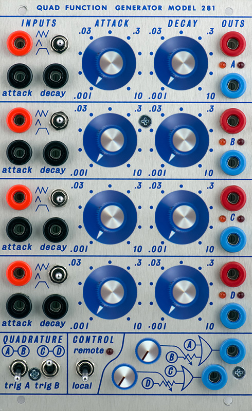
281 Quad Function Generator Module |
|
I built a V2 281 Quad Function Generator module for someone else. They sent me a mostly complete kit of parts and I assembled and tested the module. Many of the components are sourced through Mouser but specialized parts, panel, and knobs have specific sourcing requirements. See Modifications at the bottom of the page for a corrected schematic and modifications.
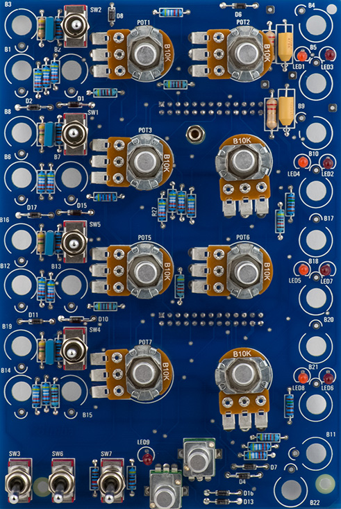
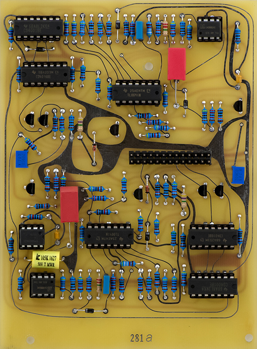
Assembly of PCB1 is straight forward.
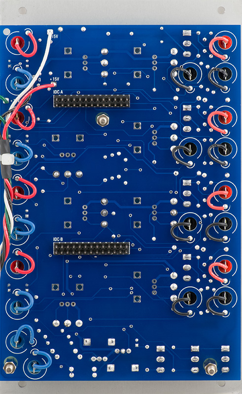
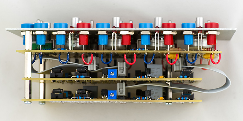
The power cable wires into discrete pads on the rear and I wire tied it to one of the connector holes.
I used sockets for the CA3080 OTAs as they are both rare and fragile.
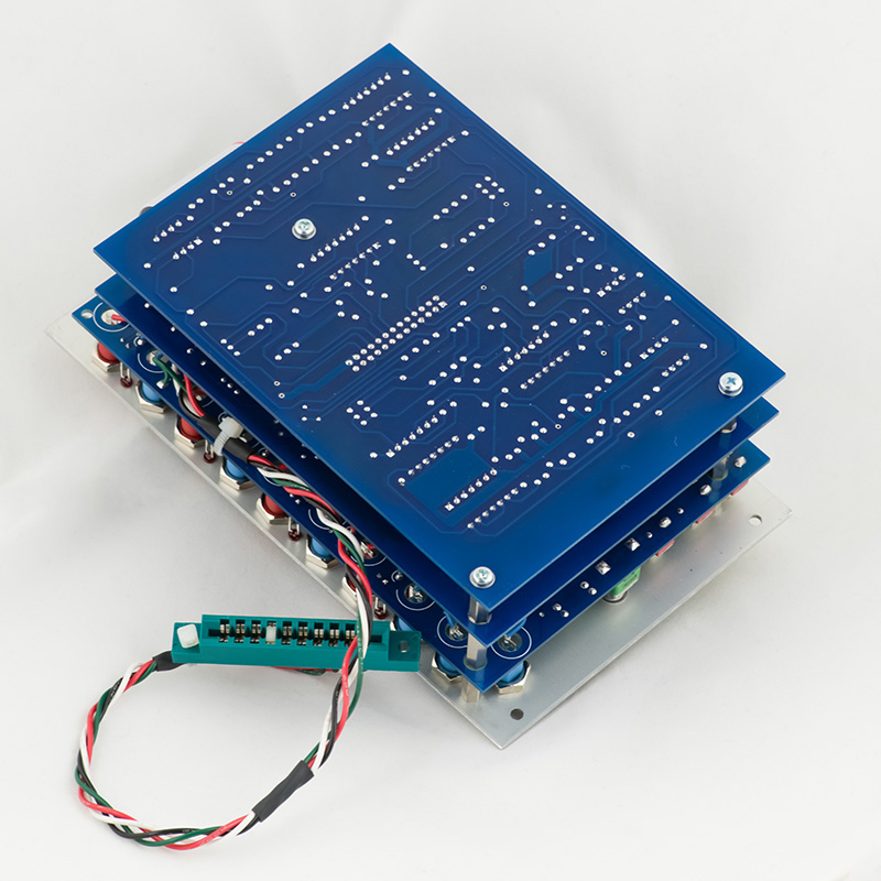
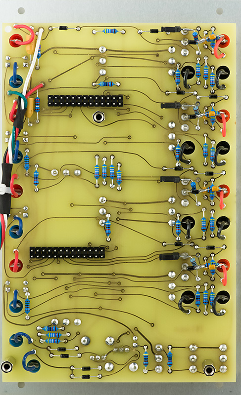
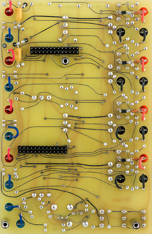
This photo shows the completed three PCB module.
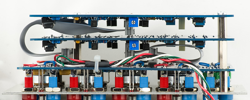
I routed the flat cables a bit different than other photos I have seen. I routed the cable that goes around the middle PCB on the side that had additional clearance. This cable needs to be split to fit around the center standoff. I made the other cable long enough that I could extend the PCB out for service. I used 20mm spacers between the panel PCB and the center PCB and 15mm spacers for the rear PCB.
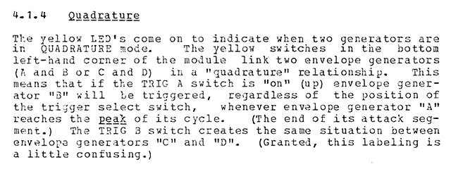
Quadrature
Quadrature mode can be a bit confusing. This explanation comes from the 1981 Buchla Synthesizer User Guide.
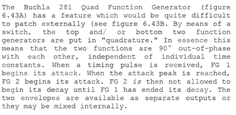
This explanation comes from the Allen Strange 1983 2nd edition of Electronic Music - Systems, Techniques and Controls.
I believe quadrature came from the desire to easily create four panning CVs for driving a 227 for quadraphonic sound. This patch consists of using all four envelope generators in quadrature mode. All four are all set to transient. A Pulse Out connects to B Trigger In, B Pulse Out connects to A Trigger in, and D Pulse Out connects to C Trigger In. Four synchronized CVs are generate that overlap for quadraphonic panning.
This view of all four CVs overlaid is a bit easer to understand.
Let's examine one pair in quadrature. Both are set to transient. B Pulse out connects to A Trigger in. When A reaches the maximum, B is triggered and A is held in sustain until B reaches the maximum. When B reaches the maximum, A starts the decay and B is held in sustain. When A reaches minimum, B starts the decay. When B reaches minimum, it generates a trigger pulse which starts the cycle over again.
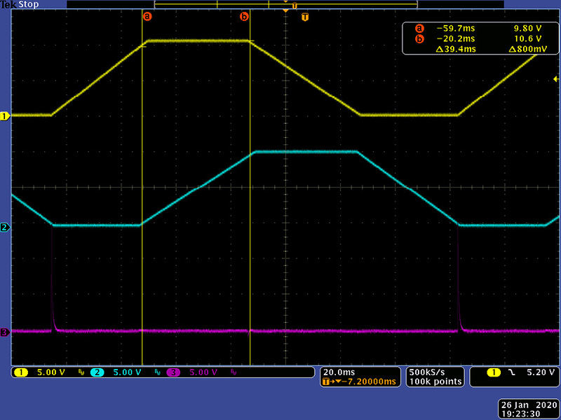
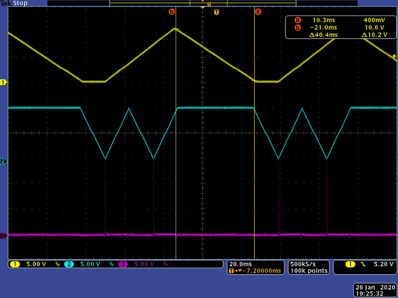
Things start to get complicated if one envelope generator is in cycle mode. This is the same setup but B is now set to cycle. B free-runs since but holds during the A decay. When A reaches the maximum it is held in sustain until B reaches the maximum (which happens very shortly with these control settings). When B reaches the maximum, A starts the decay and B is held in sustain. When A reaches minimum, B starts the decay and continues to cycle until A again reaches the maximum.
Operation
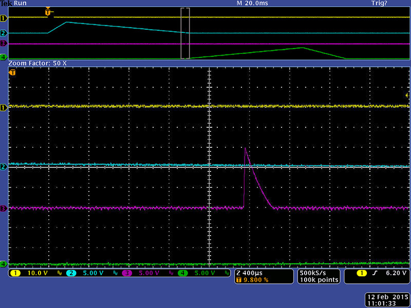
This image shows A triggering B. You can just barely see the magenta trigger pulse on this scope image.
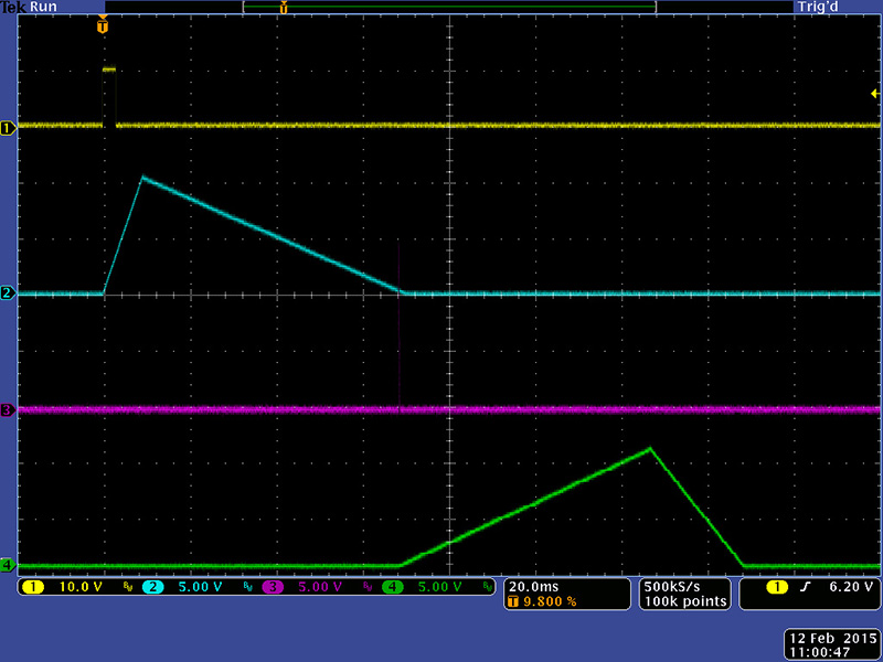
The red banana jack output is a trigger at the end of a cycle. Zooming in you can see it is a +15V pulse about 150 µS wide at mid-voltage.
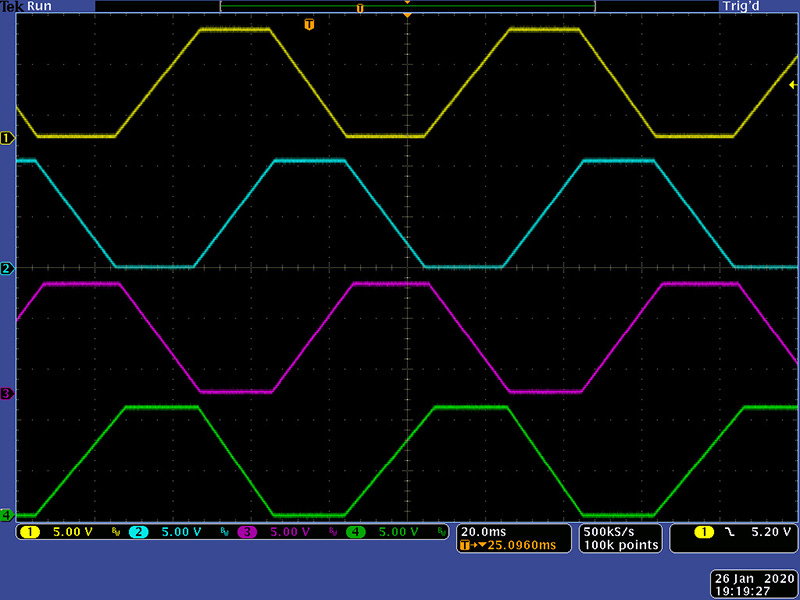
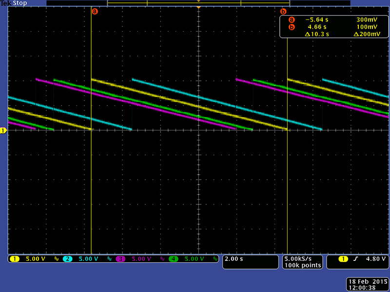
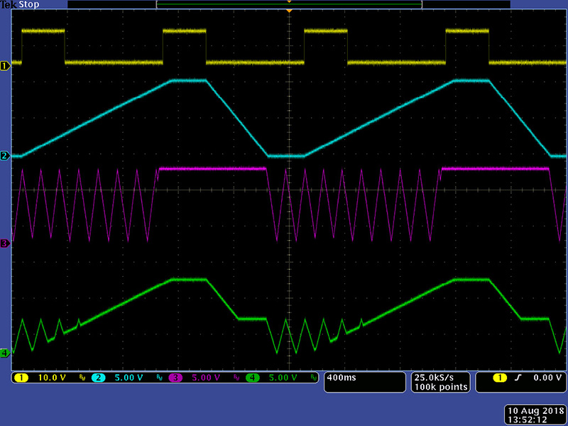
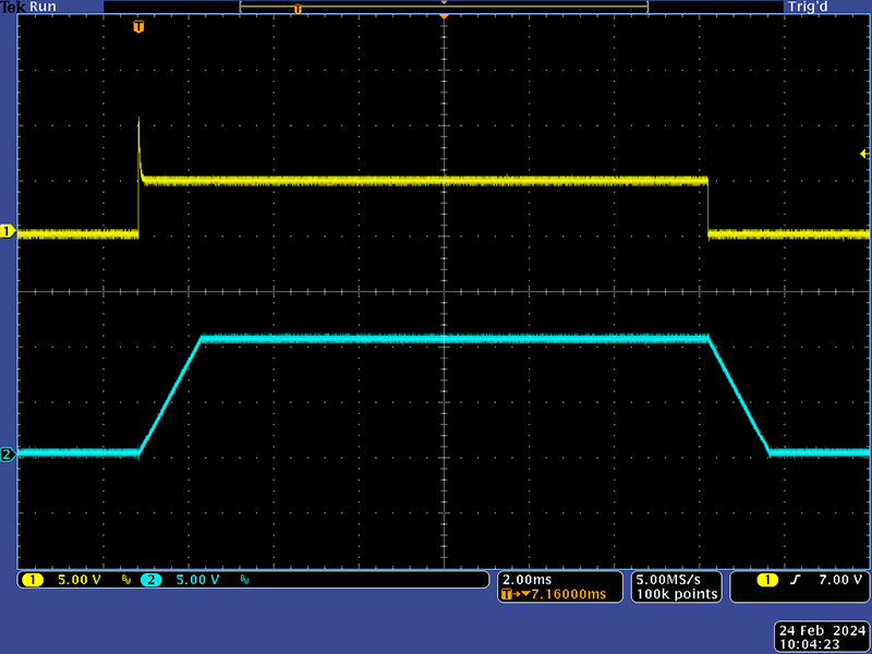
This scope image shows Out A - D in quadrature mode.
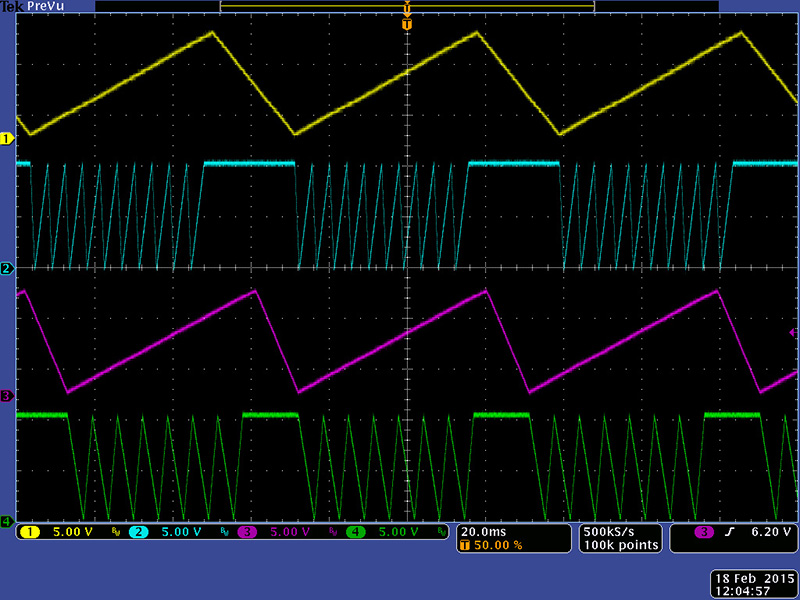
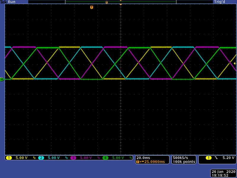
This scope image shows the same Out A and B as above and the Sum outputs.
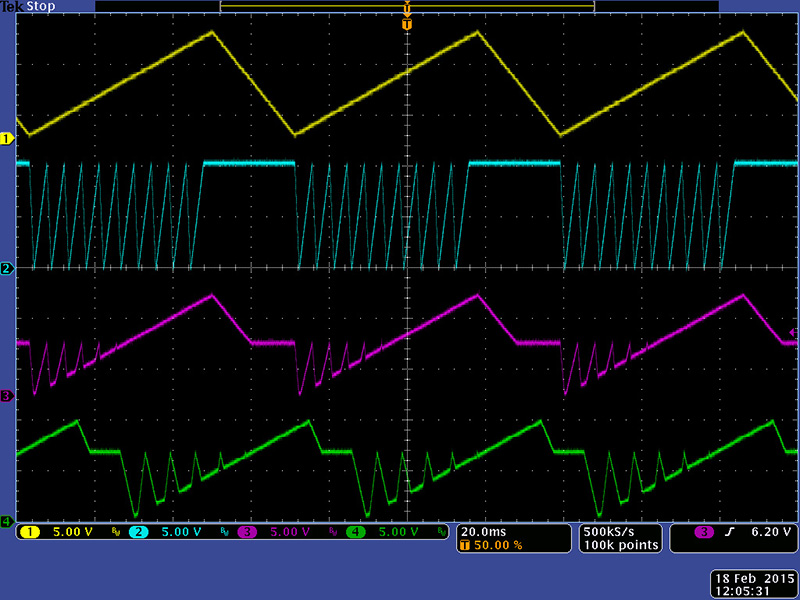
I calibrated Section A to 10 seconds and then adjusted the slope of Sections B - D to be parallel.
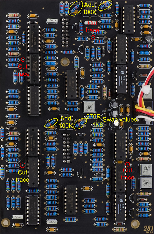
V3 Black PCBs
The V3 PCBs have a few issues that are easily corrected. The BOM for the 10V regulation resistors are swapped. R169 should be 270R and R270 should be 1K8. Pin 1 of IC7 and IC14 are driven from a saturated op-amp output through a diode. IC7 and IC14 are powered from 10V so you need a 47K resistor in series with pin 1 to limit the current. You can lift the pin and add the resistor but since the parts were in sockets, I chose to cut traces and add the resistor on the rear. All cuts are on the front of the PCB. Cut the trace to cathode of D2, to cathode of D7, right side (towards center) of R43, right side (towards center) of R109. On the rear of PCB2 add wires to connect the cathode of D2 to the left side (towards center) of R43, and the cathode of D7 to the left side (towards center) of R109 (the left side because you are working on the rear of the PCB). Then add 47K resistor from the left side (towards center) of R43 to pin 1 of IC7, and the left side (towards center) of R109 to pin 1 of IC14.

There are four op-amp inputs that are driven by diodes so they float when the diode is cutoff and noise will affect the outputs. Simply add four pull down resistors to ground. Add 100K resistors to ground to IC6 pin 3, IC6 pin 5, IC12 pin 3, and IC12 pin 5. Nearby decoupling capacitors provide ground pads.
I've also been sent a couple of modules that wouldn't cycle continuously. They might cycle for seconds or minutes but eventually would stop. What was strange is that different AC/DC adapters would either cycle or not. The LM317L has a Vin-Vout specification of 2.5V which cannot be met using the +12V supply. I lifted the input leg of IC15 and wired it over to a +15V decoupling capacitor and the module cycled correctly.
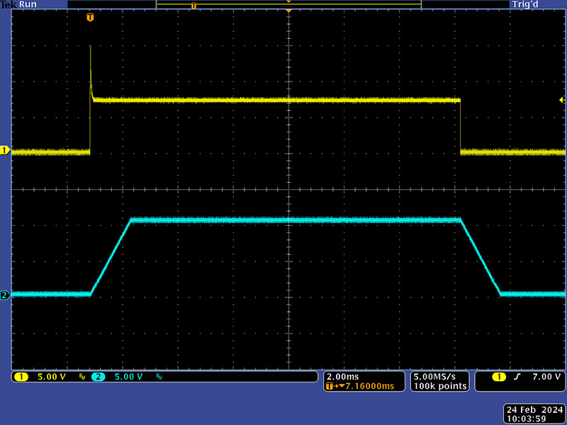
Transient mode is shown in this scope image.
![]()
This scope image shows the sustain mode where the attack is held at 10V until the input goes false.
On the V3 boards which use the THAT340 I rarely can get a full 10 seconds with the trimmers. I have sometimes simply increased the value of the timing capacitors but more recently I have changed the series resistor with the trimmer. These are on PCB2 and are R4, R12, R70, and R78. The standard value is 47K and I have used 56K, 68K or 75K depending on what was required to get 10 seconds of attack or decay with the trimmer not at either extreme.
Vintage Version PCBs
There is a hand routed version of the PCBs that is built the same as V2. It took me a while to find the reference diagrams for these PCBs which are important because there is no silk screen. I soldered the two tantalum capacitors on the rear of the PCB for additional clearance.
Transistor Q6 is rotated 180° on PCB2/3 from V2 and the 220nF capacitors (large red) and 1µF capacitor (yellow axial) on PCB2 and 3 also have wider lead spacing so I used different parts from the V2 BOM.
The 20mm standoffs are a bit tight when sockets are used as the flat cable header overlaps the IC in the socket.
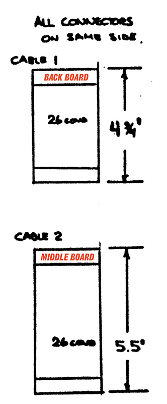
This cable diagram is from the original schematics. I do split the rear cable so it spreads over the standoff.
R69 on PCB2 is specified as 20K in the BOM but is 49K9 on the original schematic. This generates the +10V supply and with 20K the logic runs at 12.5V instead of 10V. R22 and R55 are specified as 22K in the BOM but unstuffed on the original schematic which sets the threshold for the comparator to switch from attack to decay at 10V. Both work, but I build with R69=49k9 and R22 and R55 unstuffed so the logic runs at 10V per the original schematic.
The design is very susceptible to leakage on the PCB so it has to be very clean. It is important to use matched transistors (e.g. cut tape) for Q1A and B and Q4A and B. Let the module come up to temperature before calibrating.
On one particular module, one channel would stop functioning if the Attack was set to maximum and reducing R9 from 1K to 910R corrected this.
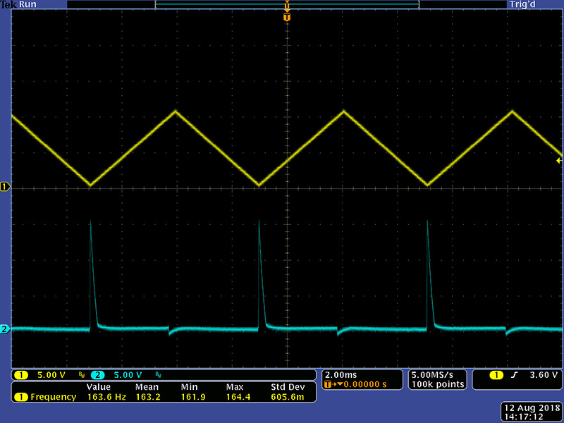
The maximum frequency was just over 160 Hz.
This image shows quadrature operation along with the A-B mixer.
Transient Mode Modifications
There are some issues with transient mode. These three alternatives provide some flexibility to the operation of transient mode.
Alternative 1 - DC Coupling (original)
There are issues with transient operation depending on the trigger/gate level. The 281 transient/sustain mode changes the input attenuator to ignore the gate portion of the trigger/gate. You want to use 1% resistors to minimize the tolerance (I always use 1% resistors as there is no real cost advantage to using 5%). As designed, it will operate with transient for a 10/5V trigger gate. Transient is still "sustained" but relies on the trigger being narrower than the attack. It also relies on the trigger amplitude being greater than 7.2V. Channels 1/3 will not correctly operate with 15/7.5V trigger/gates. The 100K resistors work correctly with 10/5V trigger/gates. However, transient will not function correctly for channels 1/3 with 15V/7.5V trigger/gates. Simply increase two resistors from 100K to 120K (R17/35 on V1/vintage and R148/165 on V2/V3). I built this PCB with the components mounted on the rear. I added jumpers to remove the DC coupling in transient mode (alternative 3) so the customer could easily select between alternative 1/2 and alternative 1/3.
These four images show proper transient/sustain with both 15/7.5V and 10/5V trigger/gates.
![]()
![]()
Alternative 2 (lower amplitude transient triggering)
The original design requires a pulse amplitude > 7.5V to correctly operate in transient. You can also "bypass" this input with a resistor/diode/capacitor to AC couple the rising edge of a pulse input which will then operate with much lower amplitude pulses. The mod consists of a diode in series with a parallel 47N/4M7 from the pulse input jack to the center pin of the cycle/transient/sustain switch. The 47N capacitor provides sufficient AC coupling and the diode blocks the negative excursions. If driving the pulse input with a module like a 245 which can drive high but not low, there is no DC path to discharge the capacitor so the 4M7 resistor provides that function.
This modification is optional and there is really no downside to installing this modification as it provides lower amplitude triggering. This photo shows the addition of the these three components between the pulse jack and the middle switch pin.
Alternative 3 - AC Coupling Only
If you do alternative 2, you can eliminate the resistors wired across the sustain switch which completely AC couples the pulse input. It will always work in transient with any pulse width and amplitude above 5V. Using a 15V gate, say from a 242, will always function correctly in transient mode (I modified mine this way).
Wire the alternative 2 modification from the input jack to the middle switch pin as shown and remove the four resistors (R14/17/32/35 on V1 and vintage, and R148/149/163/165 on V2/V3).
Pulse Modifications
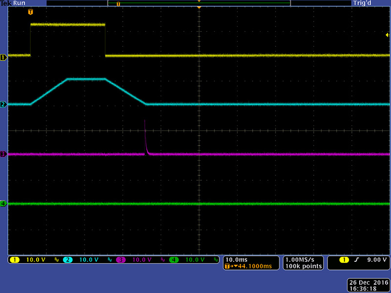
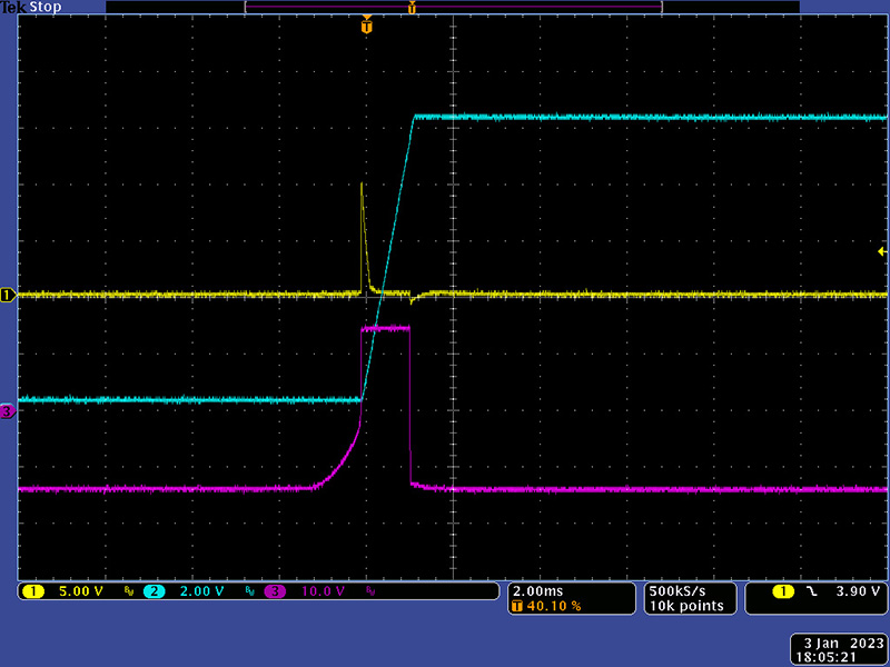
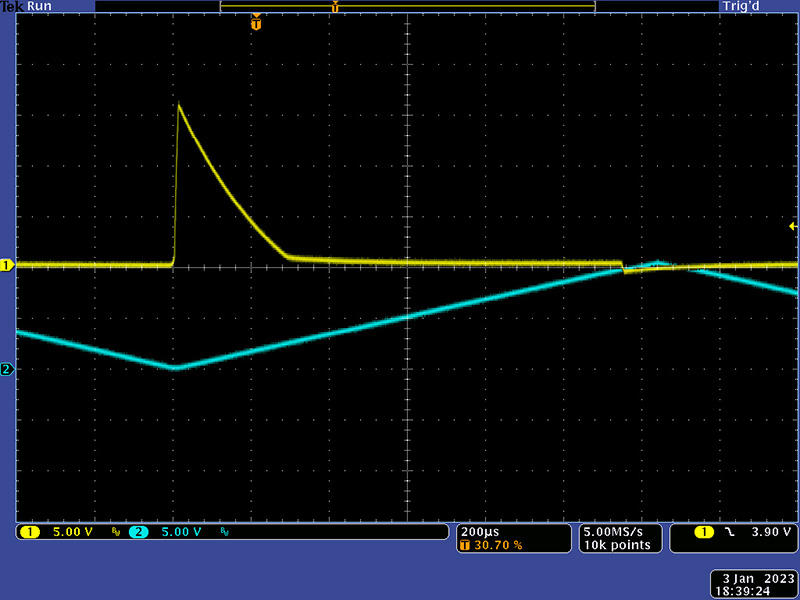
An individual contacted me about their Pulse Out decreasing in level as the Decay is increased. I could see no reason for this right off so tested my V2 281. Sure enough, as Decay increases beyond the mid position, the pulse level decreases. On these scope images, Pulse Out is yellow, CV Out is cyan, and the comparator output IC1 pin 8 or IC5 pin 8 is magenta. This image is with the Decay at mid position.
This image is with Decay at the 6th dot.
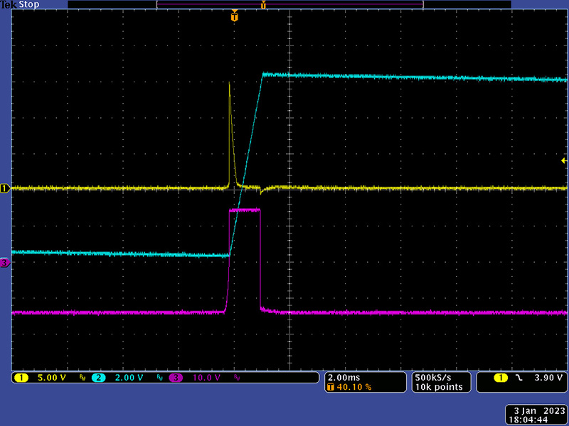
This image is with Decay at the 8th dot.
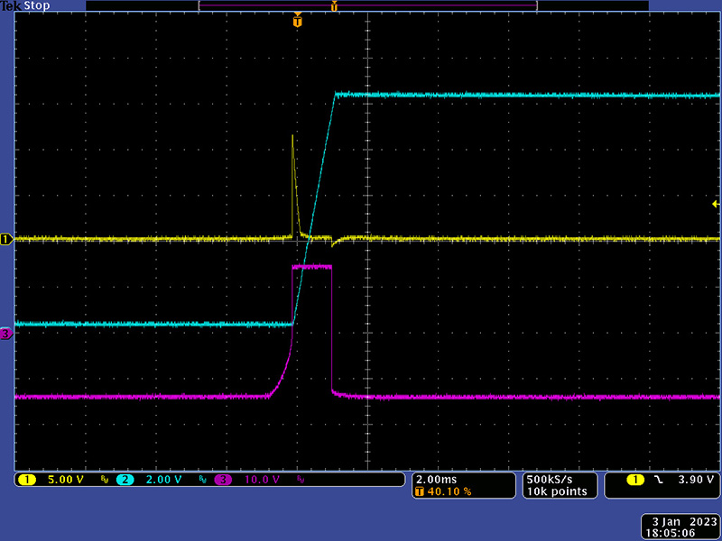
This image is with Decay on Max. You can see how the pulse output has dropped from 15V to about 11.5V.
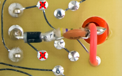
The issue is that the comparator output increases to 0V so the sharp rise that is differentiated to create the pulse is half the normal amplitude. I didn't spend any time diagnosing the root cause although I suspect leakage through the diode may be the issue. I would have designed the circuit with the hysteresis resistor connected between the output and the + input and then used the diode to block the negative voltage for the CMOS gate input. However, the circuit as designed is also over-driving the CMOS input which runs at 10V with no series limiting resistor. I simply added a second resistor between the output and the + input and it cleaned up the pulse output so called it good and I'll ignore over-driving the CMOS input since this design has been around for decades. I found a 2M2 resistor from IC1 pin 8 to pin 10 and IC5 pin 8 to pin 10 provided the best solution. This photos shows these resistors on a vintage version PCB.
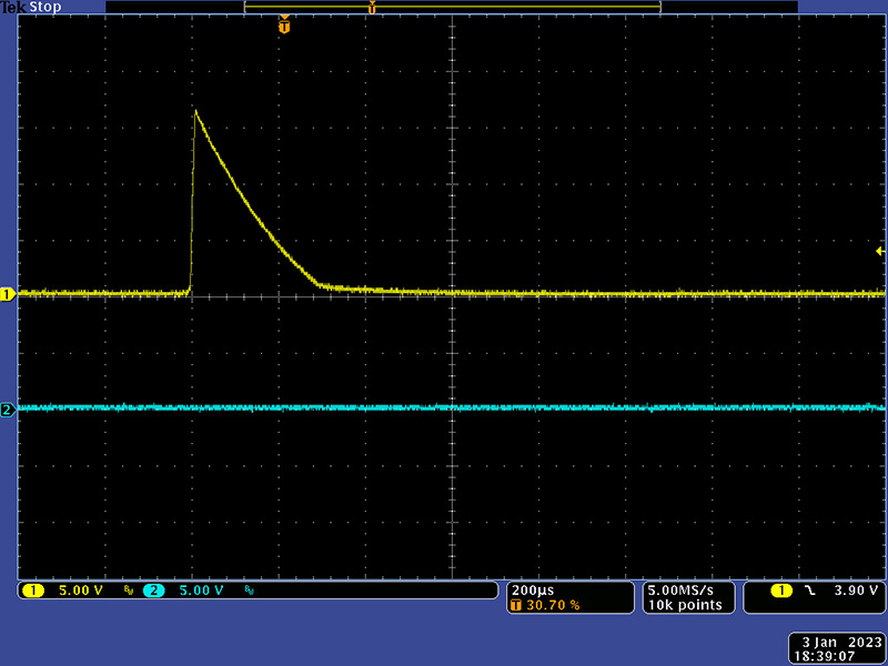
This scope image shows a 15V pulse with the Attack and Decay set at minimum (.001).
This scope image shows a 15V pulse with the Attack and Decay set at maximum (10).
Quadrature Modifications
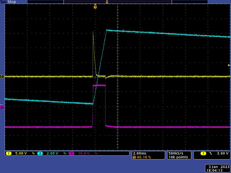
I had completed a 281 vintage build and was explaining quadrature in an email, when it didn't make sense to me. Channel 2 was terminating early as can be seen in this photo.
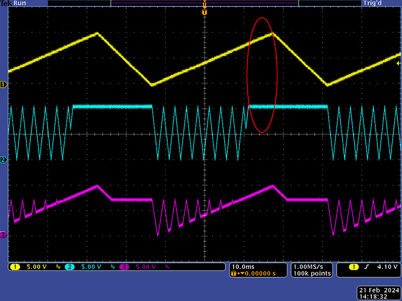
Looking at the output of IC1 pin 8 (cyan) you can see it flips state prior to the peak. Note also the output is asymmetric where the peak positive voltage is less than the peak negative voltage.
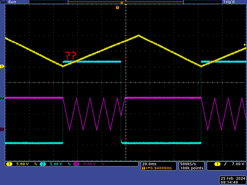
A quick check of IC5 pin 8 *cyan) shows peak voltage symmetry.
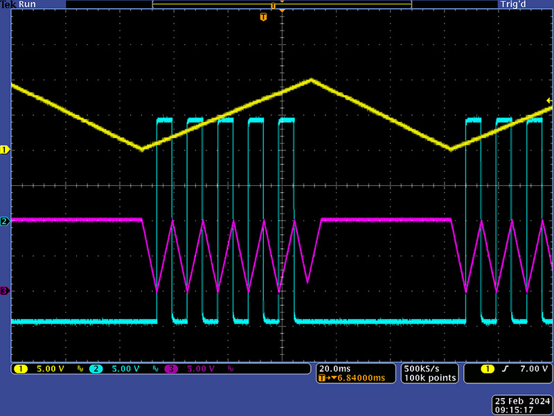
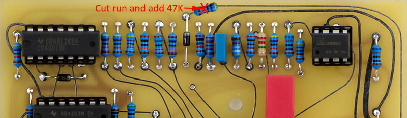
It's always bothered me that Don will over-drive CMOS inputs from op-amps. In this case, IC8 pin 1 through a diode is driving the CMOS CD4001 IC7 pin 1 directly. While this doesn't damage anything, it loads down the output of IC1. I simply cut the trace at the top of the PCB connecting D3 with IC7 pin 1 and added a 47K in series.
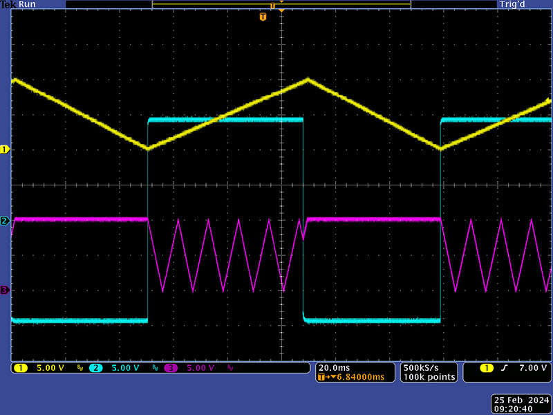
Now the quadrature thresholds are correct.
281 schematic with modifications All modifications described are included.