There are three required modifications on the Rev1 PCB and several optional
modifications that enhance performance.
-
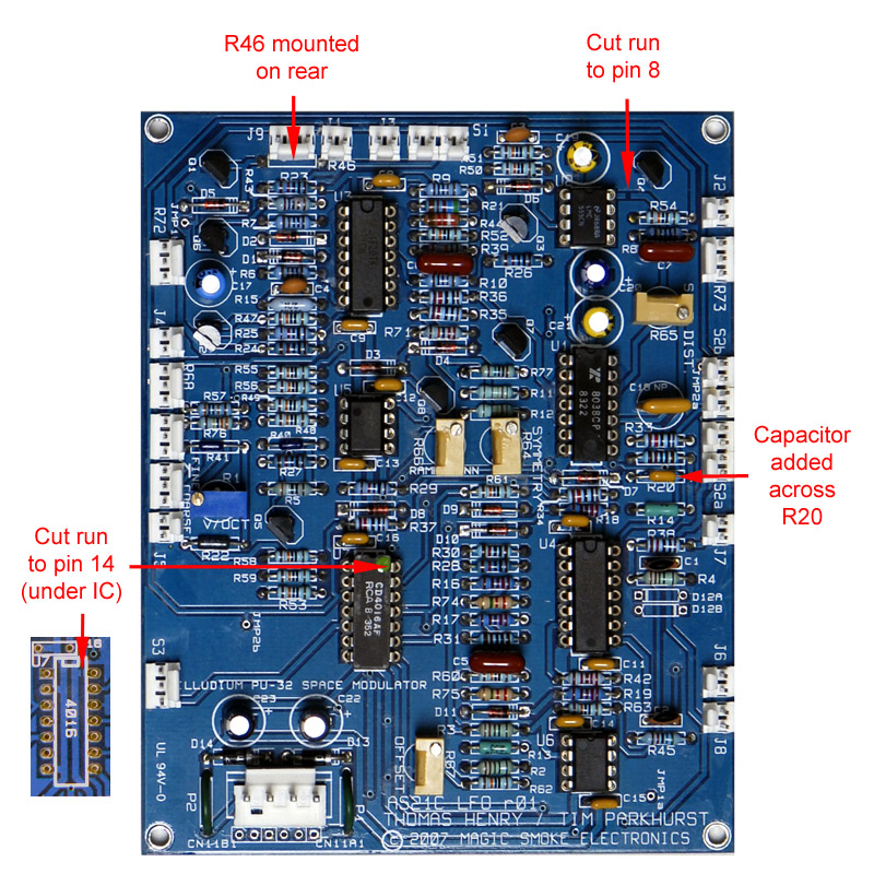
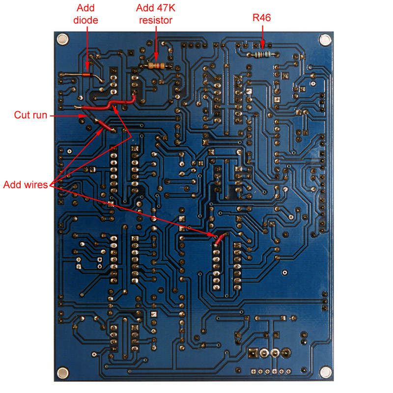
There is insufficient spacing between R46 and J9.
It is easier to mount R46 on the solder side.
-
The fast edges of the gate circuit induce slight
glitches at the peaks of the sine and triangle waves. You can see them on
a scope but they are fast enough to not cause any artifacts. I found that
by increasing R20 to 10K and paralleling a 0.02 µF capacitor it minimized the
glitches. I simply piggybacked the capacitor on R20 and is shown in
the photo.
-
The useful range of the frequency control is about -5.8
volts to +5 volts. The control range is -15 volts to +15 volts so there is
a lot of "dead" travel at each end of the control. You can change R57 to 300K
for a -5 to +5 range. You can improve the coarse control range by
changing R57 to 255K and adding a
8.06K resistor in series with the CW end of the potentiometer (between the
potentiometer and +15 volts on pin 1 of the coarse control connector). This will provide a -5.8
volt to +5 volt range.
-
The delay will false trigger if the delay trigger input is
unconnected. Normalling the jack to ground will prevent false triggering
if there is no cable plugged into the jack. I added a 47K resistor from
the base of Q3 to ground to eliminate the false triggering. I could
get some really interesting waveforms with this false triggering as each cycle
would cause a delay trigger which would truncate the current cycle for the
period of delay!
-
I often run +/- 5 volt signals into inputs such as the delay
trigger. The breakdown voltage of Q4 is rated at 6 volts so I added a
protection diode from the base to ground. This improves the margin if a negative voltage is applied to the
delay trigger input.
-
I used a 2 µF timing capacitor for the 8038 which produces a
frequency range of 0.5
Hz to 160 Hz. The sine wave holds it's shape to 0.5 Hz although the
amplitude drops off below 1 Hz. The triangle and ramp hold a
reasonable shape to about 1 Hz and then deteriorate and the amplitude
decreases below 1 Hz. Here is a 0.5 Hz sine wave with amplitude about
+/- 3 volts.
-
I found the calibration of the volt/octave a bit tricky. You
have to let the LFO temperature stabilize. The easiest way to adjust the
trimmer is to add 1 volt to the volt/oct input and adjust the trimmer for 2X the
frequency. Unfortunately this adjustment will also affect the base
frequency so you don't know the exact 2X frequency. I found it easier to
disconnected the coarse and fine controls so a 0 volts input would have 0 volts on the trimmer so it would
not affect
the base frequency. This way I could measure the base frequency at 0 volt
input and
adjust the trimmer for 2X the frequency with a 1 volt input. Then I could
check and readjust the trimmer for 4X the frequency with a 2 volt input and 8X the
frequency with a 3 volt input.