|
242M
Programmable Pulser |
|
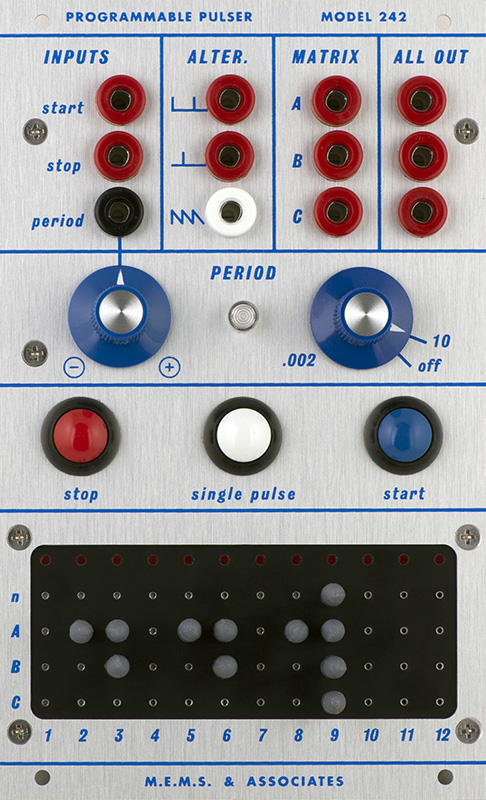
I built a MEMS 242 Programmable Pulser. This unique module will generate three distinct patterns of up to 12 pulses programmed by pins in the matrix.
A shorting pin (no diodes or resistors) into the 'n' row sets the length of the sequence. Pins in the 'A' row define a pulse to occur on that stage; likewise for the 'B' and 'C' rows. These pulses occur on the Matrix outputs.
The internal pulser is the same as the 245 with a Start, Stop, and Period CV input. The Period control sets the rate. There is no external clock input. A saw waveform is generated for each stage which can be used as a 'free' envelope output. Each All Out is a pulse per stage. They are individually diode isolated so can be patch parallel with other similar pulse outputs. The Alter(nate) outputs are gates true for the even and odd stages for the full period of the stage (the graphic is a bit misleading).
The Start and Stop control the internal clock. Single Pulse just generates a pulse that is or'd with the pulser. If running it is an extra pulse. If off then it will single step through the stages. The pulse is also or'd with the saw which will complete a ramp cycle when the button is released.
This module uses +24V so the pulse and saw outputs reach +15V.
The original module used Dialco illuminated switches which are expensive and hard to find. The Single Pulse is a SPDT momentary switch which is also more difficult to find. The circuit could be modified to operate with a SPST switch but I found these Otto P9-11312X (X=color) flush push snap-action momentary SPDT switches in the correct colors. These are not illuminated but I added a red/blue LED in a lens at the center.
Construction
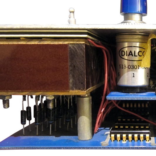
The original 242 used a Selectro #0724-0870-07A matrix board which is no longer available. The hole pattern in the bottom of PCB2A is for diodes connecting it to the matrix (this must have been fun to assemble). You can also see the Dialco switches soldered to PCB1A.
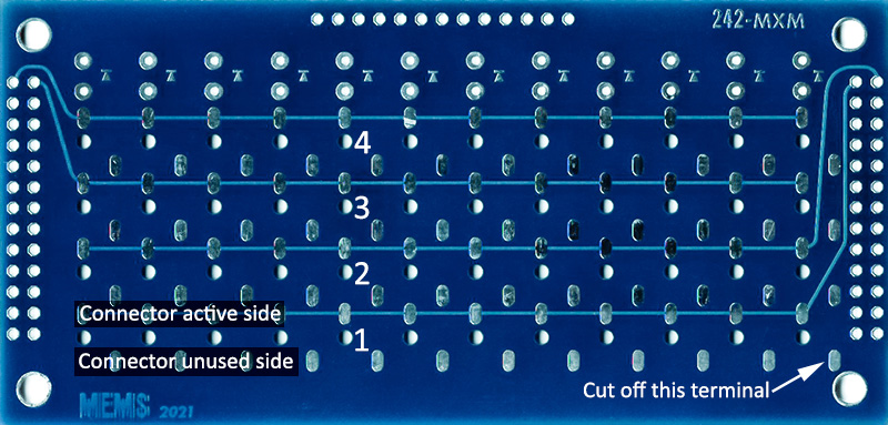
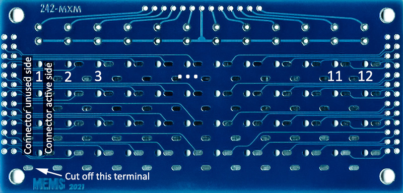
The matrix board in the MEMs reproduction is made from a sandwich of three PCBs with through-connectors oriented in the horizontal and vertical axes and a mix of thru-hole and SMT components.
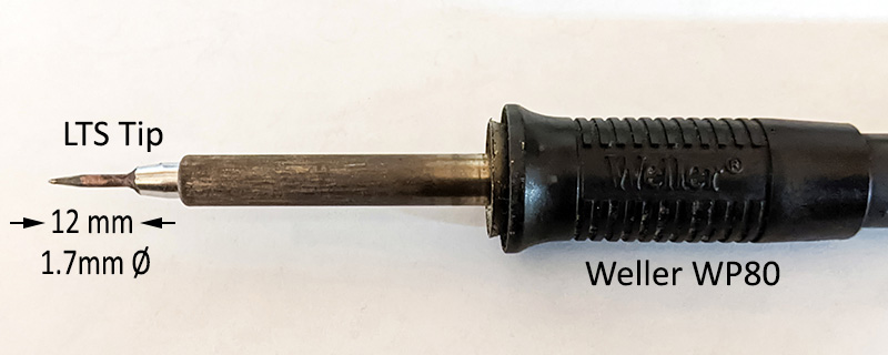
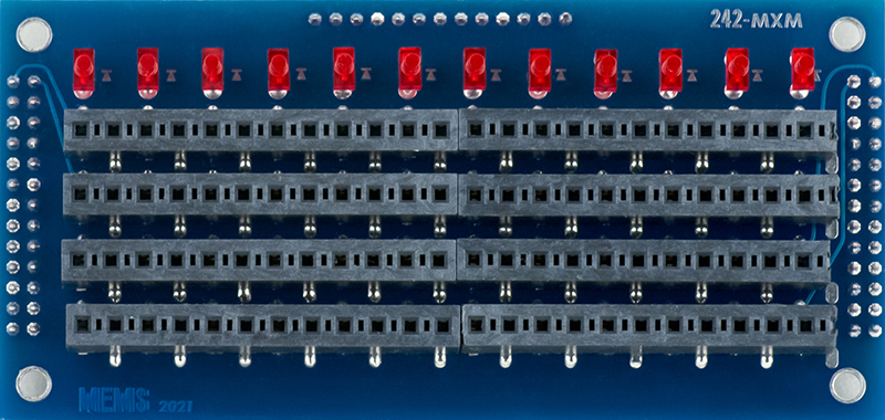
The middle PCB mounts the LEDs, horizontal and vertical connectors on both sides. The spacing is quite tight and requires a long narrow soldering tip. I found this sequence of assembly worked well.
Solder the horizontal connectors from the bottom up. This allows you to more easily access and solder the active side of the connector. Since only every other connector position is used, you need to cut off every other pin and alternate on the other side to line up with the PCB pads. The last connector position is not used and interferes with the board to board connector so I cut this position off.
Mout the panel board to the rear with 10 mm standoffs. This allowed you to insert the pins from the back to check the alignment of the connectors. Make sure the pin is perpendicular in both the horizontal and vertical orientation.
For the bottom row solder both sides of the connector. Aligned the connectors with the pad in the center of the PCB so that any error in alignment is distributed evenly to both sides.
Solder the remaining connectors in the order shown. You can only solder the active side with a normal soldering iron and tip.
I made a long narrow tip by grinding down the longest conical tip to a cylinder long enough to reach between the rows.
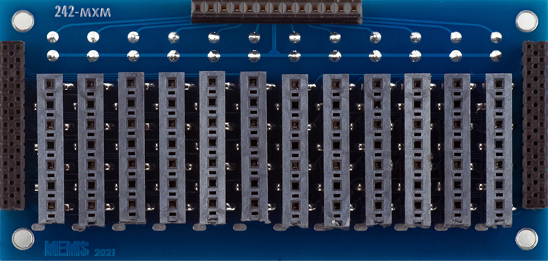
Solder the opposite side of the three rows of connectors.
Move the panel board to the front side using 10 mm standoffs.
Soldering the connectors starting from the left side which allows access to the active side of the connector. Again, only every other connector position is used so you need to cut off every other pin and alternate on the other side to line up with the PCB pads. The bottom connector position is not used so I cut that position off even though there is no interference.
Insert the pins in all four holes from the front and slip the connector on from the rear to correctly align it. For the first column solder both sides of the connector.
Solder the remaining connectors in the order shown using the pins for alignment. Again you can only solder the active side with a normal soldering iron and tip. Then go back with the narrow tip and solder the unused side.
Pull the panel PCB off and solder the female board to board connectors flush with the PCB.
Insert the LEDs and remount the panel PCB with 10 mm standoffs. Align the LED flush with the panel PCB and solder.
Wash the PCB (hopefully you used water wash flux solder). Add heat shrink around each of the LEDs leaving space at the top for the panel to eliminate bleed between LEDs. The middle PCB is now complete.
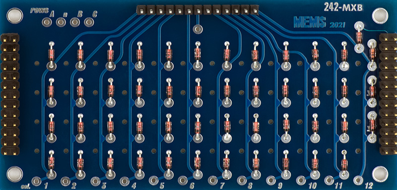
The rear board is for the switch position diodes. This completes the matrix assembly.
This photo shows the rear of the panel with the terminal strip and the small perfboard to hold the LED and resistors. I mounted the potentiometers at an angle so the resistor between the wipers would fit (the two resistors on the potentiometer are swapped in error in this photo). The completed matrix is at the bottom.
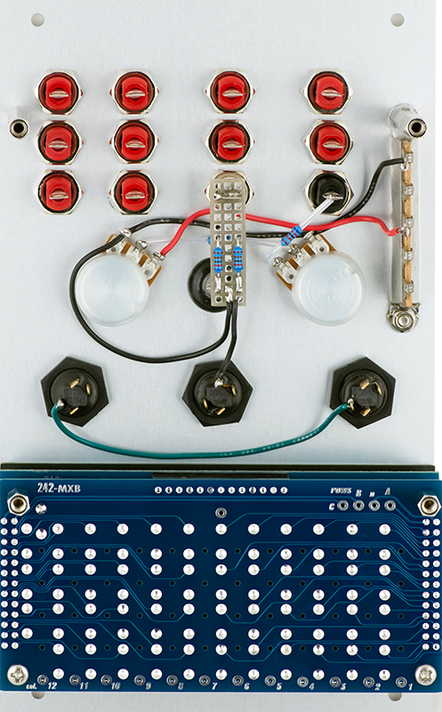
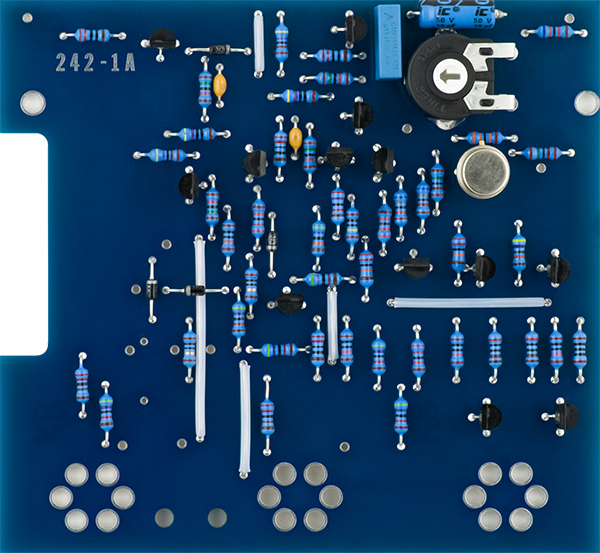
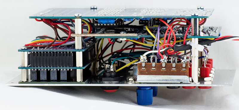
PCB 1A is the Pulser. The PCB has a notch for wiring from PCB2A to wrap around to the front panel. The Dialco switches solder directly to the PCB which makes it captive to the front panel. My Otto switches wire to this PCB so it can be removed easier for service.
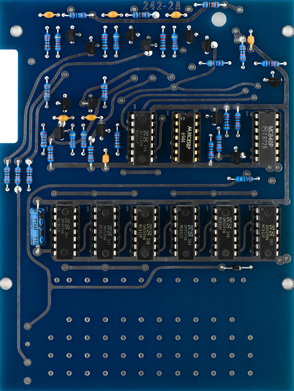
PCB 2A is the sequencer portion consisting of the JK flip flops and interface to the matrix. This design uses older RTL digital ICs. The holes on the bottom line up with the Selectro matrix. Axial diodes were wired between these holes and the Selectro matrix block.
Modifications
The pulser operates on +/-15V and +24V for 15V outputs. I do not have +24V in my system so I modified the circuit to operate on +15V. The pulses and saw amplitudes are a bit lower as a result.
I added a 15 µF capacitor after the -15V 10R series resistor (not in photo).
I added a single blue/red LED between the two controls since my switches are non-illuminated. A small perfboard soldered to the saw banana mounts the LED and adds the necessary series resistors. Two added diodes change the color to violet when the single switch is pressed.
I added an external external clock input with a three pin jumper to select the ramp banana jack as either the ramp output or the external pulse input. The threshold is 2.5V. I don't quite understand the usefulness of three separate diode isolated All Outs. I could have used one of these as the external clock input and preserved the ramp output.
The module sequencing operated erratically based on ABC pin configuration. I tied unused DTL inputs high and added decoupling capacitors to every other MC8XX IC as good design practice. A 100 pF capacitor on the "n" return line restored proper sequencing. I think the DTL Vol is 0.4V and Vil is 1.1V. The matrix diodes add 0.6V so there is only 100 mV of noise margin. There are a lot of wires which increases cross talk so I would recommend using Schottky diodes in the matrix although they are quite a bit more expensive. This increases the noise margin to 400 mV and might have eliminated this erratic behavior.
I use blue Rogan knobs for all my modules now.
Construction
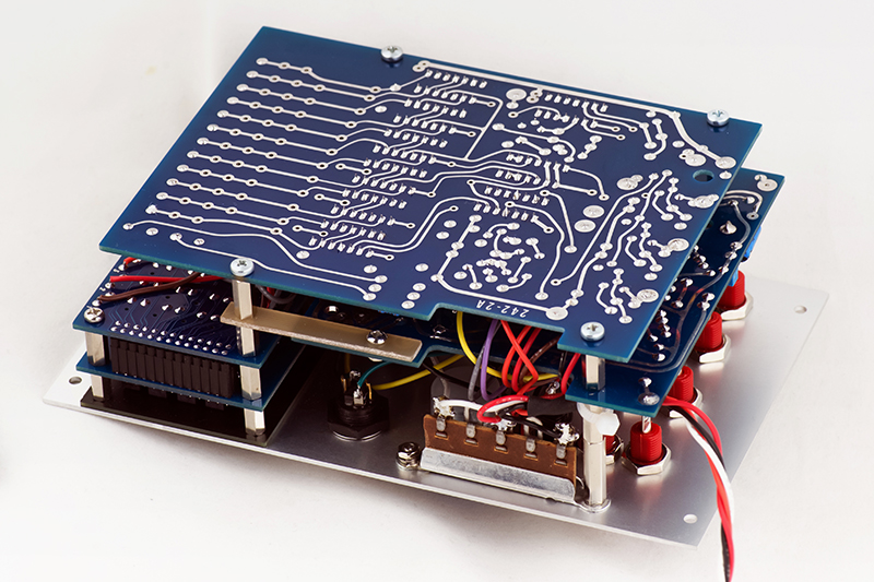
There are a lot of wires in this module. The PCB and matrix cover the entire panel. There is a notch in PCB1 for wiring from PCB2 to the front panel. There is also a notch in PCB2 which serves no purpose. In this photo you can see my two diodes for the violet color for a single press. You can also see the series resistor and diode along with a three pin jumper for the ramp output/external clock input selection.
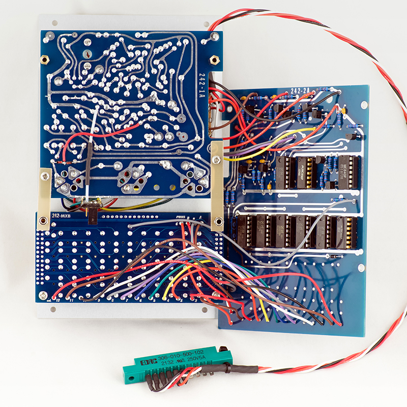
I had to make custom length standoffs for the boards to stack correctly since I did not use Dialco switches. You can see the two extensions that mount PCB1 to the standoffs. I also made a terminal strip for the power cable.
Here is the rear of the completed module.
Operations
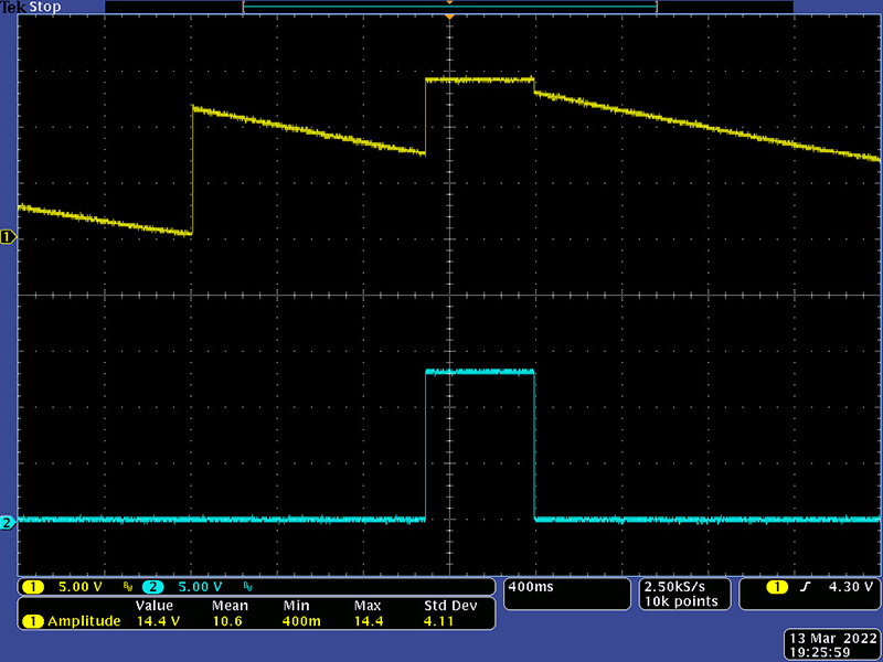
This photo shows the Ramp and All Out outputs. The All Pulse output is terminated into a 100K load.
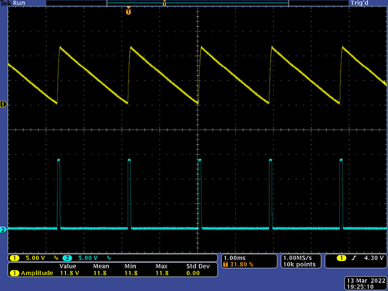
The All Out output is ~70 µS wide and ~14V amplitude.
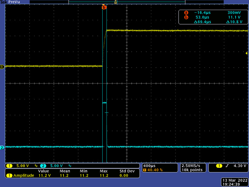
The photo shows the press of the Single Cycle button while stopped. You can see the pulse width matches the duration of the button press followed by the ramp decay based on the Period control.

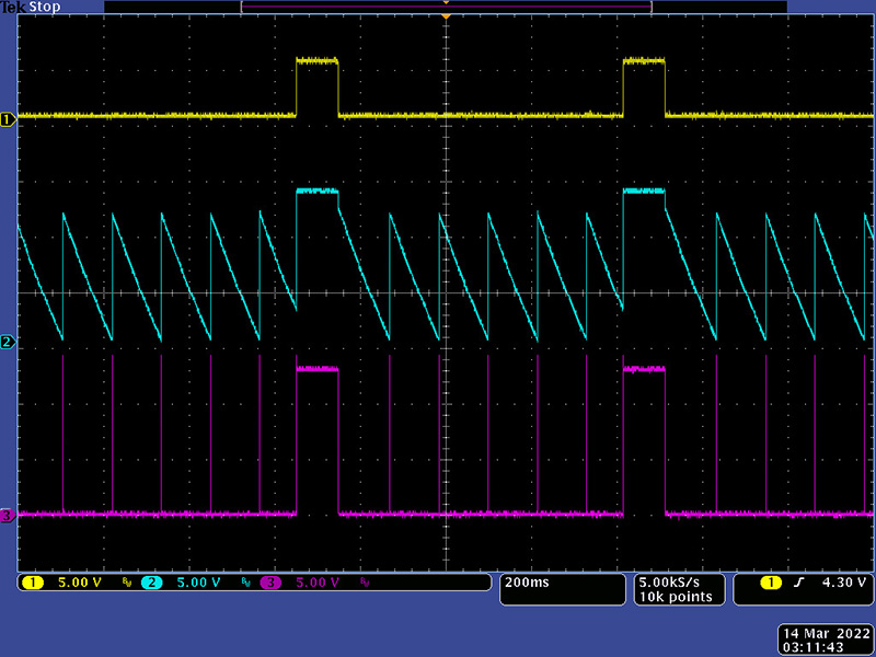
Single Cycle also works when running as this photo shows. It simply adds in the pulse followed by the ramp output based on the period control. All Out (cyan) is true for the duration of the button press.
This photo shows my modification of an external clock input (yellow) while the 242 is on. The external clock "simulates" a button press so the All Out width is the same as the clock.
For verification I made the following patch:
Set "n" to 5 and drive the 245 from the All Out (you have to single step the 242 disconnected until both are on the same stage). ABC drives a 281 EG which drives a 292 LPG. The 245 CVs drives a 244 Quantizer which drives three 258 VCOs patched to the 292 LPG.
The 245 5th pulse output drives a 244 Pulse Divider /3 which drives a 266 QRV. The 266 2n output drives a 257 (for attenuation) which drives a 244 Quantizer which drives the 258 VCOs attenuated CV.
The sequence generated a repeating 5 stage percussive pattern. The 281 Attack/Decay set the percussive effect and the 245 CVs (non-pulsed stages had no affect and could be set to minimum) set the pitch. Every 3rd sequence the VCO would transpose randomly with the range based on the 257 attenuation.