|
CEMS Clock |
|
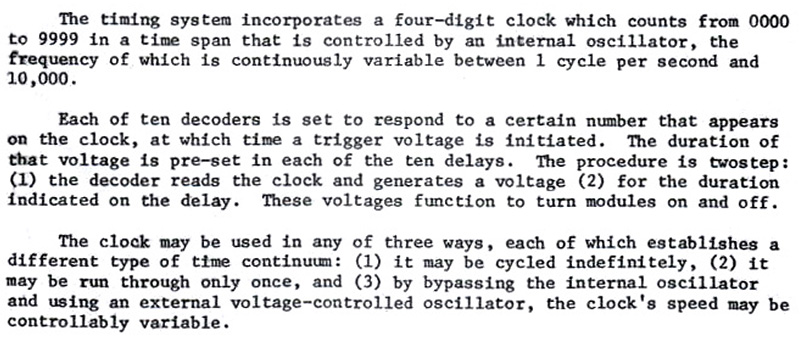
These photos are courtesy of Pasquale Rosa. This description of the clock is from the CEMS Specification.
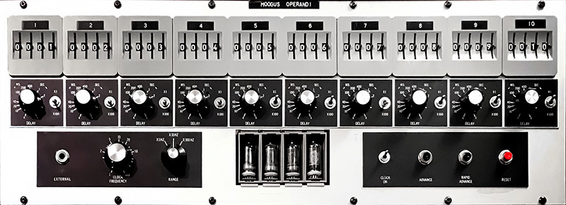
Clock (high resolution image)
This rear view of the clock shows the hand built prototype construction.
Clock rear (high resolution image)
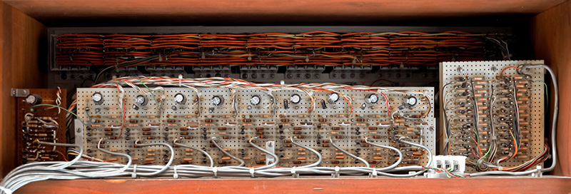
These are a number of photos with the Timing Clock removed from the cabinet. This is a rear view with the circuitry mounted on a board.
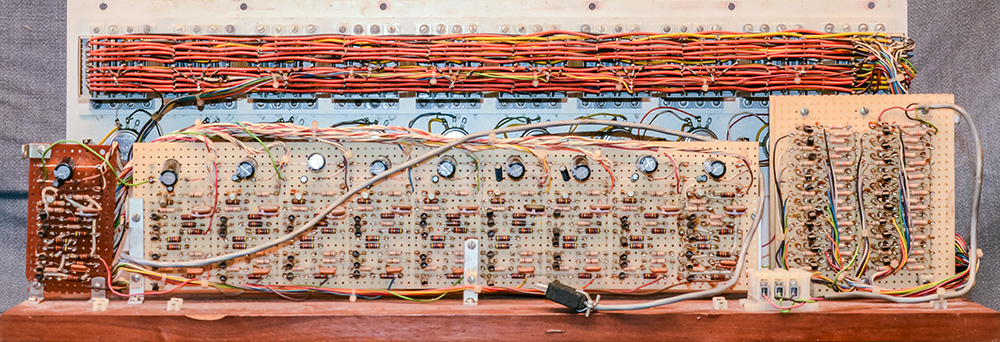
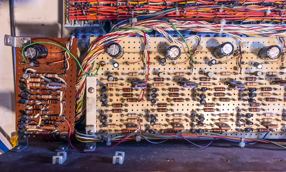
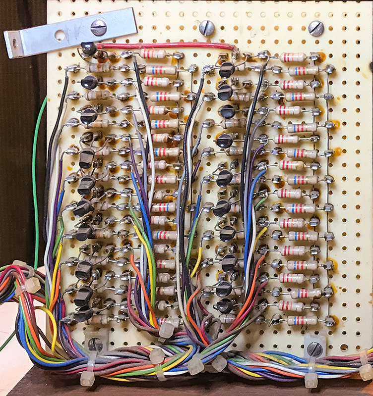
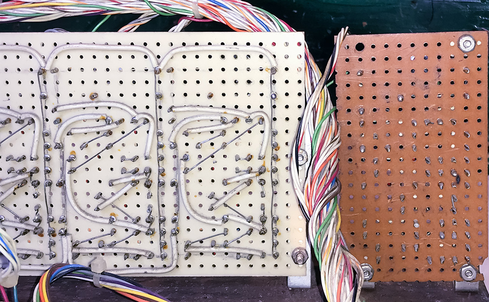
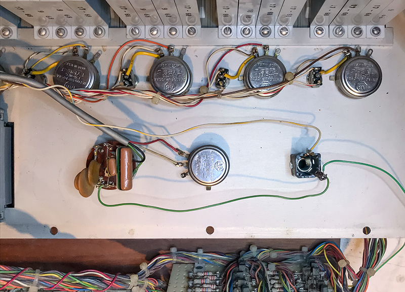
This is what I call the aux and left side of the main board.
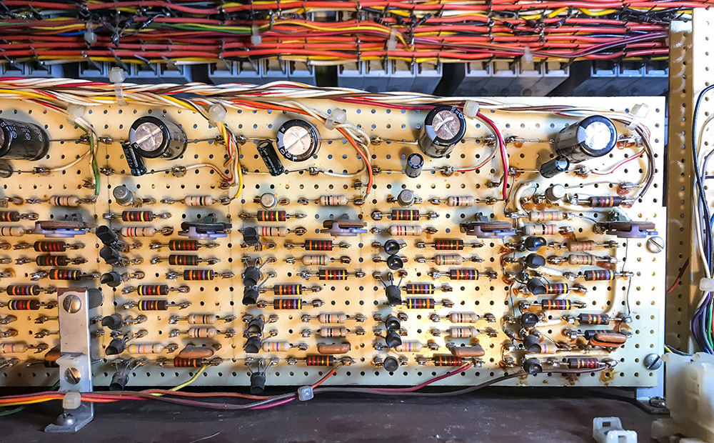
This is the right side of the main board.
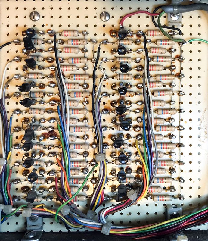
On the far right are what I call the transistor boards. Note there are two boards mounted back to back. The panel has been laid flat.
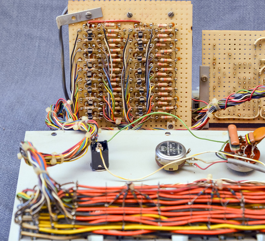
This is the component side of the inside transistor board.
This is the component side of the rear-facing transistor board.
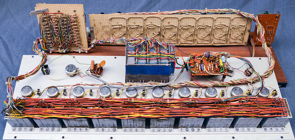
This is a view from the front with the panel laid flat.
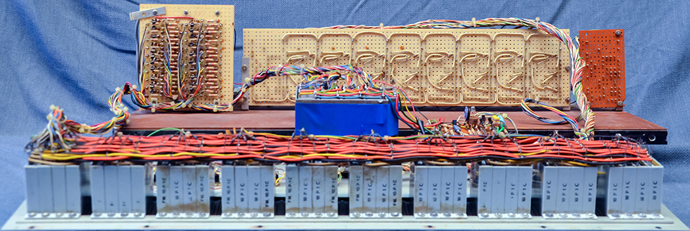
This is a slightly different perspective from the front with the panel laid flat.
This is the rear of the aux and main board left side.
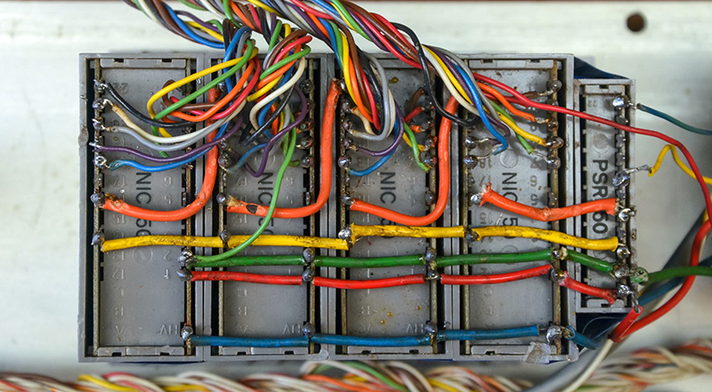
This is the front panel digit switch wiring.
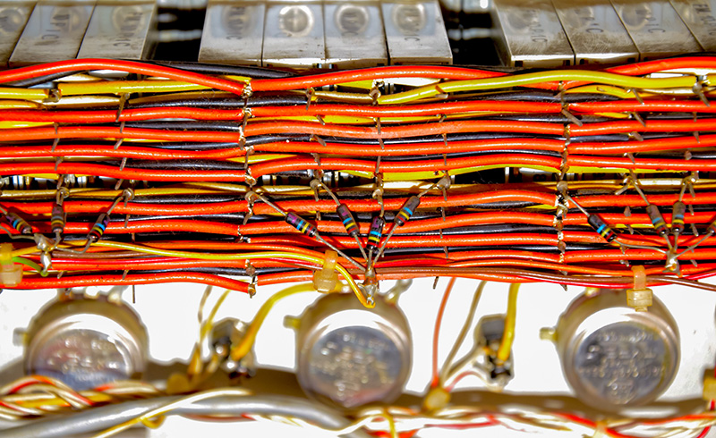
This is the Nixie tube wiring.
This is a small control board behind the right side switches.

This is a view of the panel controls with the control board lifted.
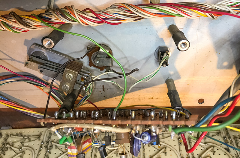
This is a view of the clock frequency and range controls.
This is a view of the range switch wiring.