|
Sputnik 244 CV Toolbox |
|
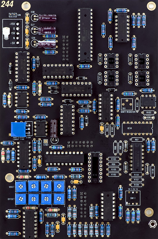
I was sent a partially built 244 CV Toolbox to finish. I programmed the AVR parts using the STK500 and an ISP adapter. Most of the controls are obvious except for the Manual Trigger. These are simple CV gate outputs controlled by the switch. The A, B, C nomenclature does not relate to the Analogue Shift Register.
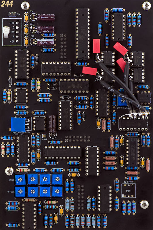
I made PCB reference diagrams from the PCB images.
Operation
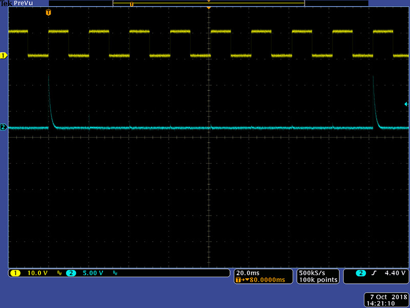
The Analogue Shift Register seems to be a very poor design. Users report offset and drift problems. I encountered both. The amount of offset is dependent on the input voltage, so you can calibrate it at one input voltage but when you change that voltage it is no longer calibrated. The outputs drift positive at a rate up to 75 mV/minute making this function impractical.
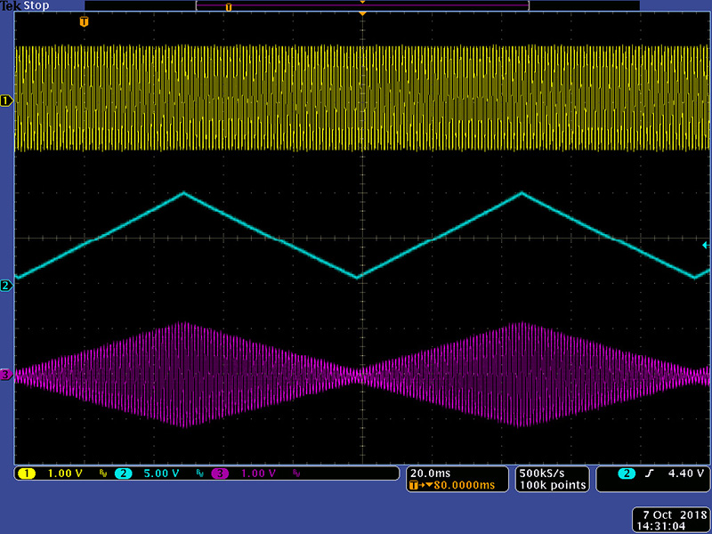
The Pulse Divider outputs 10V pulses as can be seen in these scope images. These are the /2, /3, and /4 outputs.
These are the /5, /6, and /7 outputs.
This is the /8 output.
This is the VCA output.
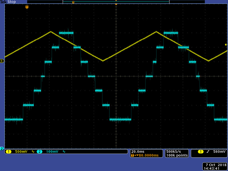
This is the Quantizer set to 1.2V/Oct. There is a bit of digital noise on the outputs, some of which may be due to my scope grounding as there isn't a convenient ground on the PCB.
Modifications
These modifications are from the build thread:
Change R17 on PCB1 from 2M2 to a jumper.
Change R117, R129, R138, and R147 on PCB2 from 4k99 to 2K (correct in the BOM)
Short pins 6 and 7 together on IC14 and IC15 on PCB2.
The manual pulse outputs undershoot upon release. I added a Schottky diode to correct this. Connect the cathode to the top of R14 and the anode to the bottom terminal of SW5. Do the same for R15/SW6 and R16/SW7.
Calibration
Calibration is straightforward.
Clock the Analogue Shift Register at about 10 Hz and set the difference between the In and C output to 0V with TR1.
Calibrate the V-Ref pad to 2.56V with trimmer TR4.
With no input, adjust each Quantizer output to 0V with the Offset trimmers TR3, TR6, TR8, and TR10.
Apply 6V to each Quantizer input. Adjust each Quantizer output to 6V with the V/Oct trimmers TR2, TR5, TR7, and TR9.
ASR Epilog
I've investigated the increasing voltage drift from the analog shift register and how to improve it. There are four S&H cells. The input signal is multiplexed to one of the four S&H cells and the outputs are demultiplexed to the three outputs. A CD4052 is used which means the input voltage has to be between 0 and 15V. Since the input range is +/-13.5V the input signal is reduced to 45% and then offset to remain within the 0 to 15V range of the CD4052. The outputs of the demultiplexers then need to have the offset subtracted and the gain increased by 2.2X. The output stage is inverting which is why droop results in an increasing voltage drift.
There are numerous weaknesses in this design. While the input stage gain is trimmable, the output stage gains are not and 1% resistors can result in a gain error of up to 2%. In addition, one stage may be high by 2% and another low by 2% so channel to channel can be off by 4%. The input and output offsets likewise use 1% resistors so have the same error range. The input and output op-amps also have offset voltages. Any droop in the S&H cell is increased 2.2X due to the output gain.
My offset and gain modifications consisted of changing the input IC12 to a TL072B and the output IC20 to a TL074B to minimize offset in lieu of trimmers. I then changed the 10K 1% resistors R97, R102, R103, and R108 to 10K 0.1% and the 22K 1% resistors R99, R100, R101, R106, R107, R110, and R111 to 22K 0.1%. Note that also the four CA3140s do not have offset trimmers. Total offset through the path amounts to around 10 mV or so.
The signal path from the multiplexer to the S&H capacitors to the CA3140 inputs is critical and needs to be short with ground guards around the signal. The PCB was designed with no special consideration for the S&H circuit. I lifted the multiplexer outputs, S&H capacitors, and CA3140 inputs and wired them together with shielded coax.
Ground for the shield is found on IC14 pin 8. Connect these pins
together:
IC14 pin 1 - bottom of C34 - IC16 pin 3
IC14 pin 2 - bottom of C38 - IC18 pin 3
IC14 pin 4 - bottom of C40 - IC19 pin 3
IC14 pin 5 - bottom of C37 - IC17 pin 3
I measured the modified 244 "C" output voltage drift over 15 minutes.
| Time | "C"Output drift from start |
| Initial | 0 (reference) |
| 1 minute | +5 mV |
| 2 minutes | +8 mV |
| 3 minutes | +13 mV |
| 4 minutes | +16 mV |
| 5 minutes | +20 mV |
| 10 minutes | +44 mV |
| 15 minutes | +72 mV |
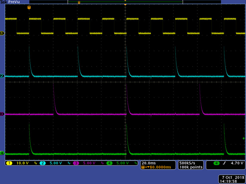
The output drifted 72 mV over 15 minutes, or 4.8 mV/minute. On a 1.2V/Oct system, a semitone is 100 mV so this represents a drift of 4.8 cents per minute. However, over 15 minutes it represents a drift of 72 cents. This is significantly improved over a different unmodified 244 but is still significant drift. The S&H cell outputs are reasonably stable but additional drift is coming from the CD4052 demultiplexers.
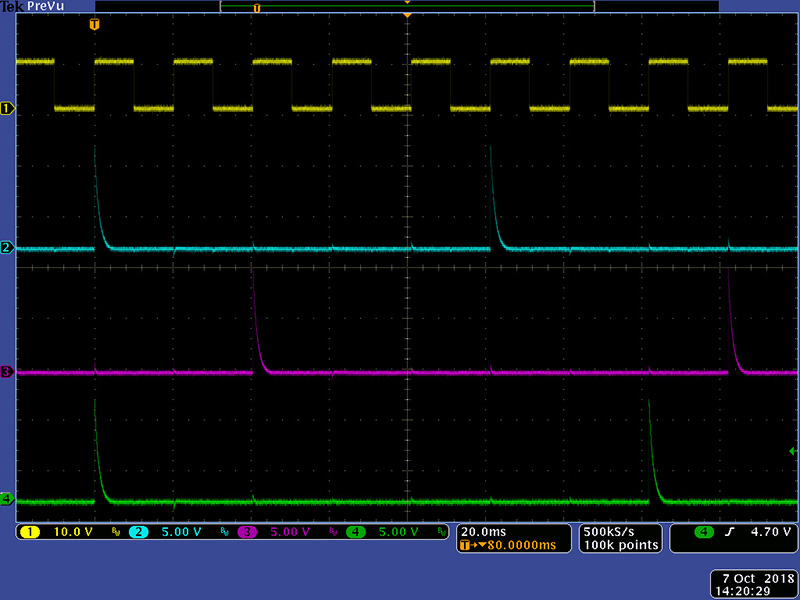
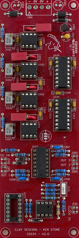
Mike Peake modified a 244 using a CGS-34 V2 PCB. The topology of this design is much better using a bipolar multiplexer/demultiplexer which eliminates the offset and gain errors and provides unity gain through the circuit. The layout is also well done minimizing droop. I powered a CGS-34 V2 from +/-15V and made the same measurements.
| Time | "C"Output drift from start |
| Initial | 0 reference |
| 1 minute | -3 mV |
| 2 minutes | -5 mV |
| 3 minutes | -6 mV |
| 4 minutes | -7 mV |
| 5 minutes | -9 mV |
| 10 minutes | -12 mV |
| 15 minutes | -13 mV |
The CGS-34 V2 has significantly less drift so modifying the 244 by adding a CGS-34 V2 provides significantly better results.
Prepare PCB2 by not installing/removing these parts:
Remove R95 - R109 (15 resistors)
Remove TR1
Remove IC14 - IC19
Replace C33, C35, C36, and C36 with a link
Note IC20 needs to be installed to generate the -5V. The
three links are for the unused sections.
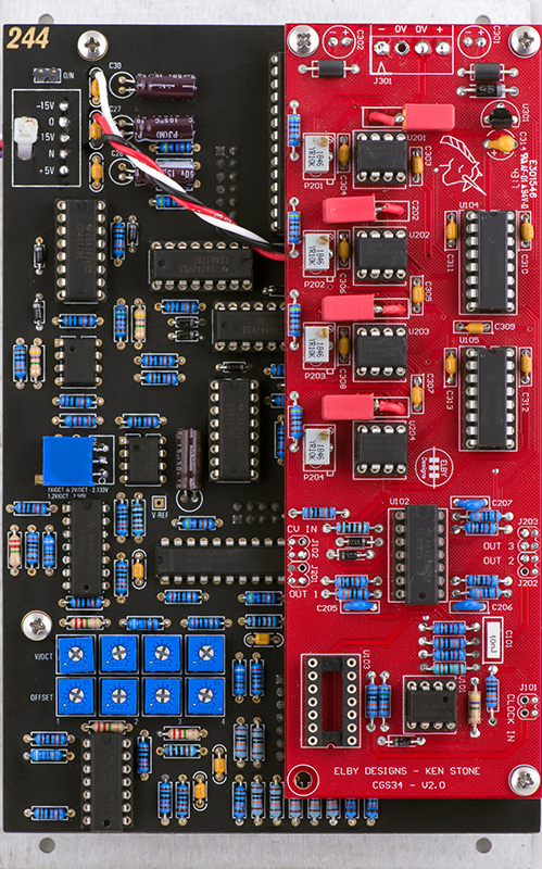
This image shows PCB2 prepared. I did not remove sockets except for IC14 as I needed to solder wires to pins 9 and 10. I drilled a hole in the bottom right corner to line up with the CGS board which will be mounted on the right side.
I used the trigger and counter circuit on the 244 to drive the CGS-34 so U103A must be removed. This counter is operated from +5V. The counter on the 244 is operated from +15V so the Q0 and Q1 outputs will be 15V. The DG409 can accept inputs up to Vcc+2V so will operate fine with these higher voltage inputs.
This board was already built so I did not remove additional parts from it. Some parts are mounted flat and on the rear to minimize the depth of the module.
If the CGS-34 V2 is built then you need to remove U103A as shown in the photo.
If the CGS34 V2 is not built, you can also leave these parts out.
R101 - R108
D101
C101
U101A
U301, D301, and C314 (note this removes the local +5V which
must be supplied from the 244)
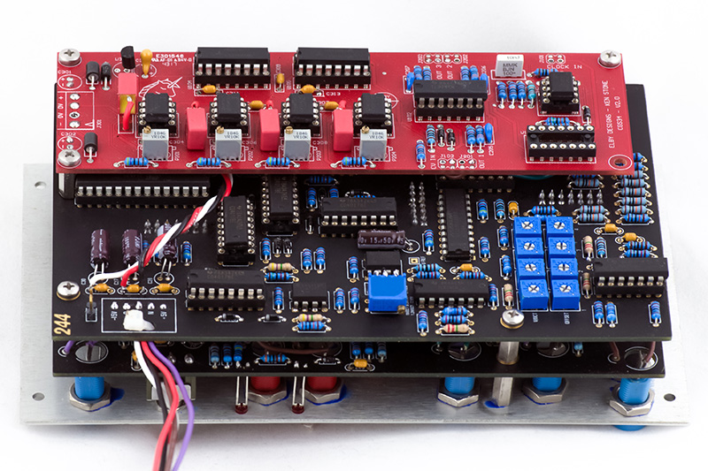
Although the CGS-34 is designed for +/-12V it works fine on +/-15V. Wire the +/-15V and Ground CGS-34. If you did not install the local +5V then wire +5 to the left pad of C314.
Wire the CGS-34 J102 to the bottom of R104
(signal input)
Wire the CGS-34 J201 to the bottom of R98
(A Out)
Wire the CGS-34 J202 to the left side of R105
(B Out)
Wire the CGS-34 J203 to the left side of R109
(C Out)
Wire the CGS-34 U103A pin 12 to IC14 pin 10 (Q0)
Wire the CGS-34 U103A pin 11 to IC14 pin 9 (Q1)
The top left CGS-34 standoff doesn't screw to the 244 and is filed to fit around the IC. The depth of the module is 50 mm.
Quantizer Epilog
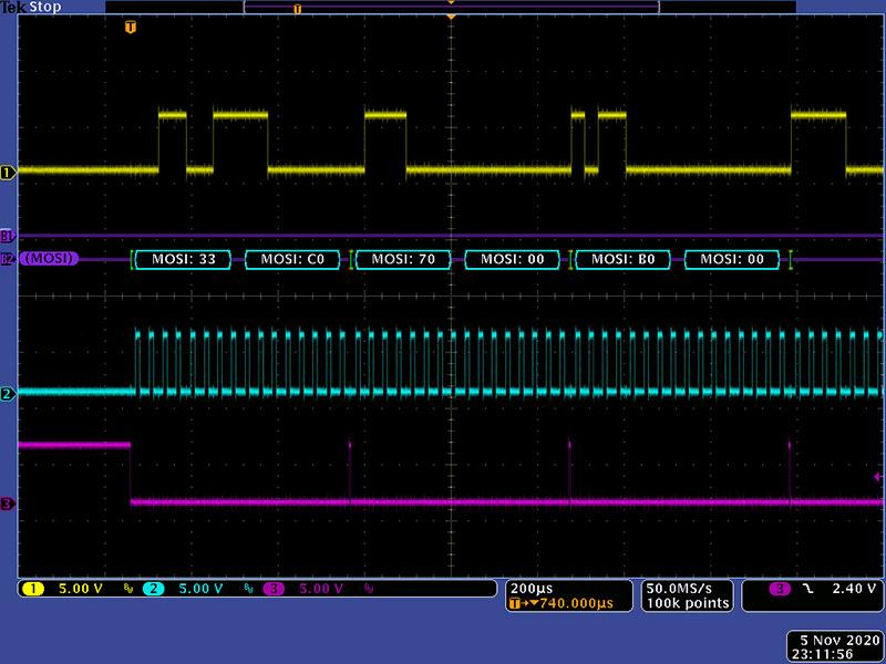
I needed to do a repair on a quantizer. The voltage increments made no sense. I couldn't tell if the A/D on the ATTINY84A was bad or the DAC on the MAX5250 was bad. I ended up decoding the SPI communications between them to see if it made any sense. The first word $33C0 is a load input register A to 240 and update all DACs.
It turns out it was a bad etch on the PCB. I see more of these types of problems on the black/gold PCBs.