|
246
Sequential Voltage |
|
I was sent a 246 to modify similar to my 245 Sequential Voltage Source modifications.
I made reference designators from PCB images. The components cover the silk screen legends once populated which makes it near impossible to find components.
PCB1 Rear Reference Designators
PCB2 Rear Reference Designators
Modifications
The original 246 used a 24V supply and the logic was a mix of DTL and early TTL that ran from +5V. This redesign uses CMOS with a 15V supply and the 24V circuitry is simply driven from 15V with no compensating changes. In addition, a number of resistors were changed or added.
I modified a 245 and 246 and my customer's email back was "So the report is - they work flawlessly. Null zone has been reduced to almost nil, adjacent stage pulse outputs now individually trigger the 281's - even three/four in a row. I encountered no problems with the stage trapping - either open ended on either side or between two mid-points."
These modifications are the same as for the 245 so see my 245 Sequential Voltage Source page for detailed information. This page simply consists of the component reference numbers for the modifications specific to the 246.
Stage CV Input
PCB2:
With 16 stages there are no unused gates with floating inputs.
Add a 100 pF capacitor across R65.
Stage CV Output Level
PCB1:
Remove R27, R28 R29, and R31.
PCB2:
Change R294, R296, R298, and R317 to 330K.
Remove C57, C58, C59, C61.
Remove R279, R280, R281, R282, R283, R284, R285, R286, R287, R302, R303, R304.
Remove Q75, Q76, Q77, Q79.
Connect the base to the collector with a link on Q75, Q76, Q77, Q79.
Replace R288, R289, R290, R307 with a link.
Replace IC31, IC32, IC33, IC34 with LT1637.
Swap pins 2 and 3 of IC31, IC32, IC33, IC34.
Stage Pulse Output Level
PCB2:
Change R55, R61, R72, R78, R86, R92, R100, R106, R114, R120, R128, R134, R142,
R148, R156, R162, R170, R176,
R184, R190, R198, R204, R212, R218, R226,
R232, R240, R246, R254, R260, R268, R275 to 6K8.
"e" (internal stage clock) Waveshape
I adjusted the waveshape similar to the 245 but the baseline
sits at 4V, not 2V (I believe) due to the number of stages. When I changed all the stage pulse output resistors to 6K8 the module would no
longer advance. I simply adjusted the clock waveshape trimmers until it
functioned reliably.
PCB2:
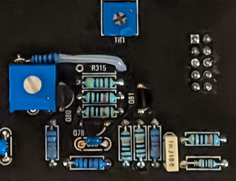
Change R301 to a 10K trimmer.
Change R306 & R315 to a 10K trimmer (wiper at the node connecting R306 &
R315).
I've worked with a number of people by email. They found they had to do the diode modification (Epilog below) and this slightly different modification to the "e" waveshape.
PCB2:
Change R306 and R315 to 10K trimmers
Adjust R315 for a baseline of 2V. Adjust R306 for an 8V amplitude above the
baseline.
Pulser Output
PCB2:
Change R30 to a link/wire.
Remove R42.
Reference Output
PCB1:
Change R3 to a link/wire.
Remove R5.
Additional modifications may be needed and are detailed in Epilog1 below. Some modules require this and some don't. I've never taken the time to do a root cause analysis to fully understand why.
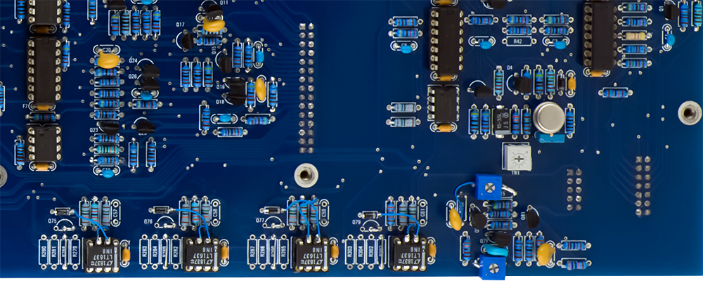
This image shows my original "e" waveshape and CV output modifications on PCB2.
This image shows all the modifications to PCB2.
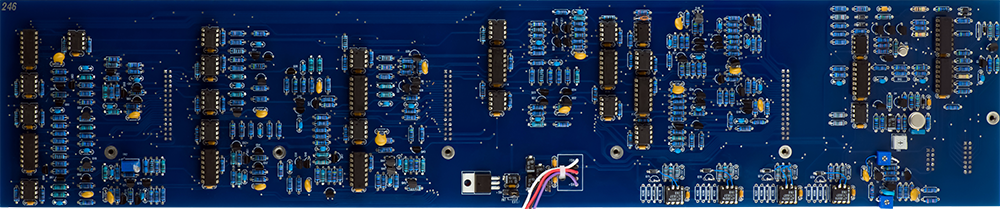
PCB2 modifications photo (larger PDF)
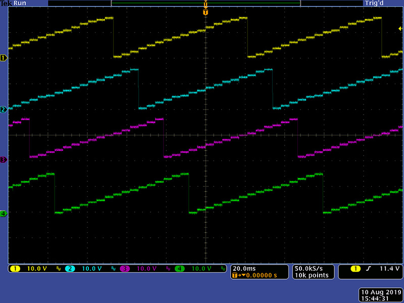
Here are the four CV outputs with a full 0 to 15V range.
Calibration
The "e" waveshape I calibrate based on operation. These sometimes stall with all the outputs at maximum so I adjust my added "e" waveshape trimmers for reliable operation.
The legends never match operation and it is important to use a 10K pot for the proper taper. I make sure it is never faster than 2 mS and sometimes adjust C4 a bit lower to make sure it doesn't stall on the longest setting.
TR2 sets the tracking of the Analog input. This takes a bit of explanation. First, the values used in the BOM are different from the original. Second, the notes on the schematic for the 245 and 246 conflict. On the 245 there is no trimmer. On the 246 there is a 27K and a 5K trimmer. This, plus the additional 11 1K stage resistors is a bit less than the 43K2 resistor used in the 245. Third, it says to calibrate Stage 16 for 14.5V but this string can't adjust greater than 6.5V. In addition, the Analog input op-amp can't pass more than about 13.5V, so you can't have a threshold at 14.25V. Note that Roman change the gain of IC21 from -0.366X to -1X which changed all these thresholds. To understand what the stock voltage thresholds of the 246 please see my 245M page.
The Analog input over-rides the pulse input. Therefore, 0V input, as in nothing connected, would constantly select Stage 1. The Analog input has to be slightly positive to select Stage 1 which allows pulse operation with no Analog input.
Now comes in the difference in BOM values. To keep all the stage select intervals the same, the sum of R63 and R80 should be 1K. R63 sets the minimum positive voltage to select Stage 1. Next comes the decision about what the stage intervals should be. The Analog input op-amp can't drive higher than 13.5V, so 16 stages would be 0.844V which is an odd value. If you picked 0.5V your maximum CV would be 8V. If you picked 0.75 your maximum CV would be 12V, a bit higher than some 10V modules can drive. Another choice might be to select a 10V range which is a 0.625V interval. Let's work through the values for that.
With 1K stage resistors, you want a string current of 625 µA. You probably want your thresholds a bit lower, so we can set the first stage at 0.425V. This allows 200 mV of margin when trying to drive it with a 10V CV. At 625 µA you want the sum of R63 and R80 to be 680R. You probably want the positive voltage to set Stage 1 of 100 mV, so R63 should be 160R and R80 should be 523R. The top resistor, which is the 100K trimmer is adjusted to about 8K32.
Note this is theoretical as I have not tweaked the stage resistor values on the modules I have worked on.
Epilog1
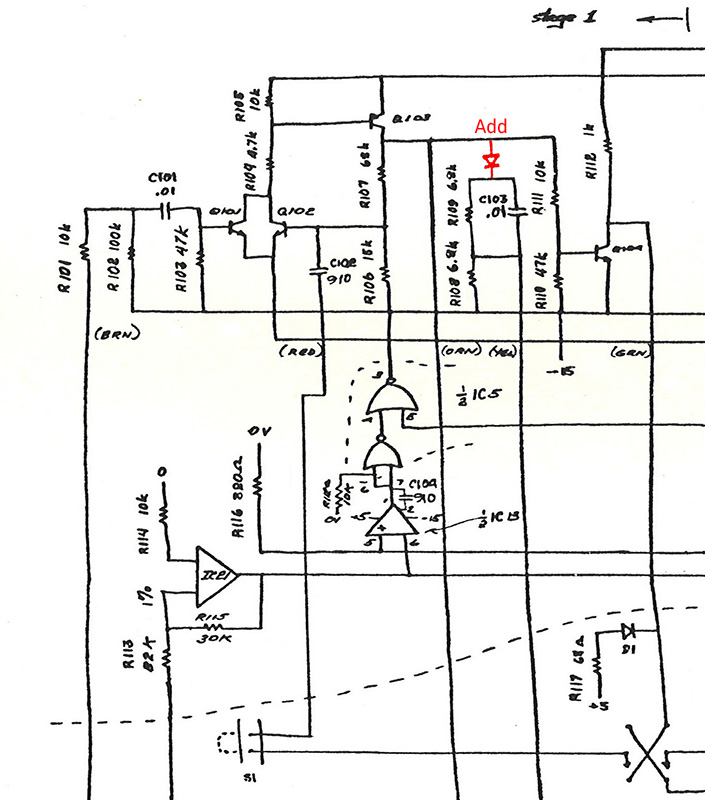
I had a 246 come in for service that would not advance at all. Individual stages could be addressed. In looking at the individual stage timing I noticed something quite odd. The green is the emitter of Q101/Q102 which resets the stage. Magenta is the collector of Q102 rising to turn off Q103. Yellow is the collector of Q103 which then falls as all stages are reset. Cyan is the base of Q102 which shows it reverse biased to turn it off. What is odd is the collector of Q103 drops to about 4V and then slopes down. It never gets low enough to turn off Q104 which creates the pulse to turn on the next stage. Thus is simply sits on the current stage. These reference numbers are for the original schematics. On the 246r Q11 is Q103 for stage 1.
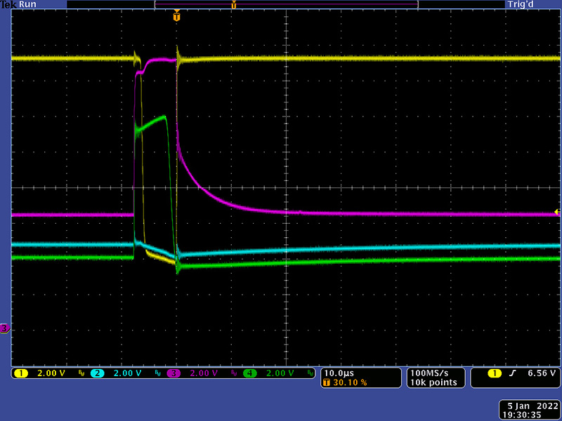
For some reason, C103 is holding the collector voltage high as Q103 turns off. In this image I have removed Q102 and am simply driving the base of Q103 with an external source. Note the long RC decay once the collector drops to 4V. This is an asynchronous machine and the reset has to occur before Q104 turns off so it can set the next stage.
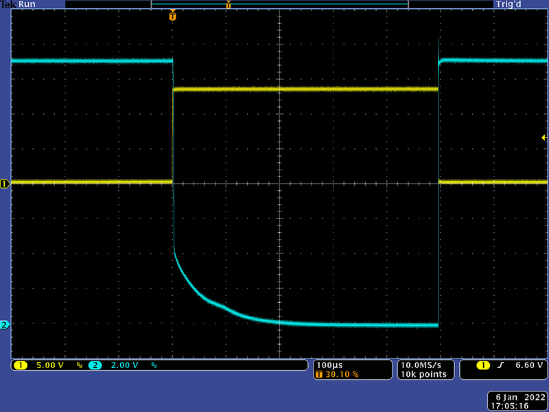
These modules are hard to work on and the board was not washed. I never could track down in a reasonable timeframe the root cause of this issue. One alternative was to significantly load the collector of Q3. A 1K resistor to ground pulled the waveform to 0V fast enough. However, this adds a 15 mA spike in current and these modules are finicky enough already. This image shows proper operation with these 1K resistors.

Another alternative would be to replace R108 and R109 with 510R resistors. This did work but I didn't want these current spikes so I did not pursue this further.
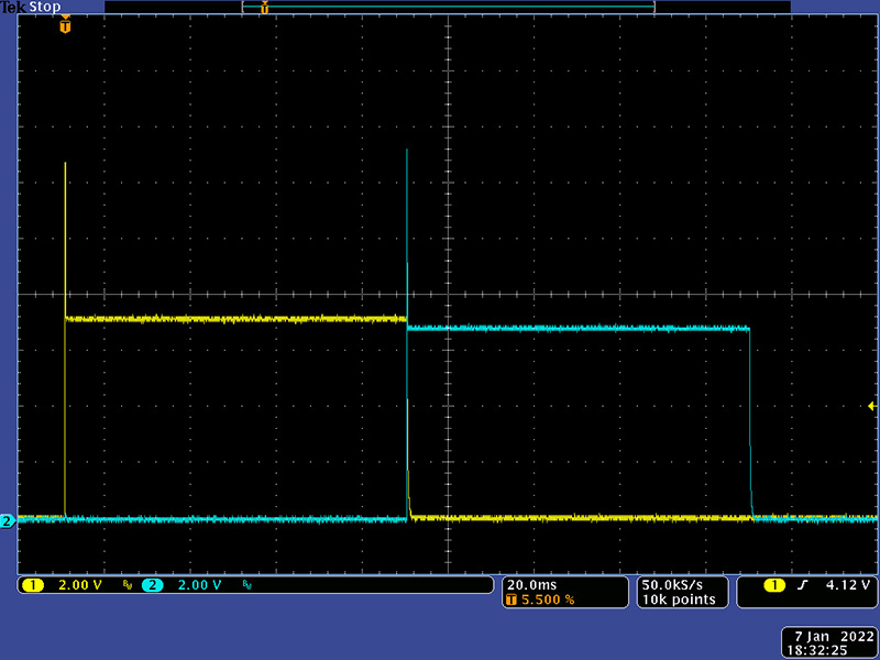
What I ended up doing was diode decoupling R108/R109/C103. I simply lifted the end of R109/C3 that connects to the collector and added a signal diode. This worked great. This image photo shows the yellow stage with the 1K resistor and the cyan stage with the diode. You can see the diode drop of about 0.4V in the gate level. The trigger is actually a bit higher because Q103 isn't loaded as much. Although the diode adds a drop, remember these were originally built with 5% resistors so the gate level could be off by 10% depending on tolerance build up. These levels are fine as-is.
Here's the diode modification I did to all 16 stages. I've helped others by email with similar situations where this mod resulted in reliable operation.
I'm having more and more people contact me with this issue. I wish I had dug deeper to figure out a root cause of why some do and do not have this issue. Here are the instructions for the modification. You have to lift the end of the resistor and capacitor that connect to the collector of the transistor. Bend the parts to connect the leads together and add either a Schottky or signal diode with the anode in the pad from either the resistor or capacitor. Wire the cathode to the lifted parts. These are in order of the stages. If you think you have this issue, you can always modify 2 or 3 stages and see if normal operation is restored for them.
| Stage | Resistor | Capacitor | Transistor |
| 1 | R55 | C9 | Q11 |
| 2 | R72 | C12 | Q15 |
| 3 | R86 | C15 | Q19 |
| 4 | R100 | C18 | Q23 |
| 5 | R114 | C21 | Q27 |
| 6 | R128 | C24 | Q31 |
| 7 | R142 | C27 | Q35 |
| 8 | R156 | C30 | Q39 |
| 9 | R170 | C33 | Q43 |
| 10 | R184 | C36 | Q47 |
| 11 | R198 | C39 | Q51 |
| 12 | R212 | C42 | Q55 |
| 13 | R226 | C45 | Q59 |
| 14 | R240 | C48 | Q63 |
| 15 | R254 | C51 | Q67 |
| 16 | R268 | C54 | Q71 |
A customer sent me information on which leads to lift. Click on the image to see a full size PDF.
Epilog2
This details a previous modification which has been replaced above with two trimmers. It his here for historical information only. There are photos and calibration description as the end of my 245 page. This module would stall with all 48 controls turned to maximum. I did a slightly different "e" waveshape modification. The R301 trimmer does very little so I left it as 15K. I instead used a 10K trimmer with the CCW and center for R306 and added a 1K resistor between CW and R315. This seemed to work better.

A 3/8" flat trimmer fits nicely over C62 if you bend it over. You can solder two trimmer leads directly to the pads and bend the remaining lead to the top to solder the 1K resistor to it.