|
256 Dual Control
Voltage |
|
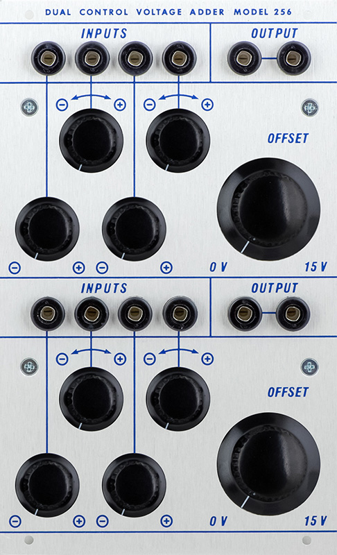
I built a 256 Control Voltage Processor module for someone else. They sent me a complete kit of parts and I assembled and tested the module. Many of the components are sourced through Mouser but specialized parts, panel, and knobs have specific sourcing requirements. Here is a photo of an original module.
The BOM does not specify six 0.1 µF decoupling capacitors (Mouser 581-SA105E104M) nor the four 15mm FF standoffs (Mouser 534-24395). There is only a single PCB in the module.
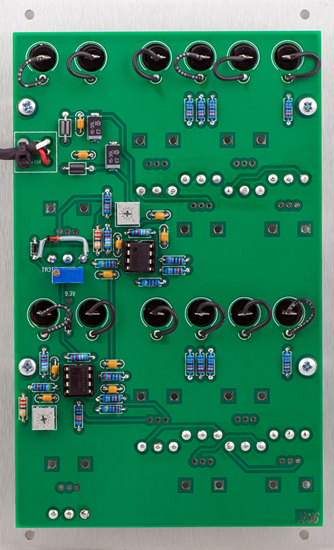
The Alpha 16mm potentiometers are very close together and any twisting of the potentiometer when tightening to the panel will short to the adjacent potentiometer. I used heat shrink on the full length of six pins to provide adequate insulation.
![]()
I slightly unbent the leg to slide on the heat shrink, then bent the leg back so the heat shrink would fit flush to the phenolic. Be sure to hold the potentiometer pin when bending so no stress is applied to the phenolic. These potentiometers are only soldered on the middle pin since I have not yet attached the panel. I securely fasten the panel, then reflow the center pin to relieve any stress, then solder the outer pins.
![]()
Operation
TR1 and TR2 adjust the output offset voltage. Make sure the panel offset control is turned fully CCW and then adjust the trimmer for 0V output. The front panel Offset control only adds 0 to 10V so the 15V panel nomenclature is wrong. The gain of the first stage is 0.5 and the gain of the second stage is 1.36 so 15V(0.5)(1.36)=10.2V. If you want the offset control to go 0 to 15V then change R15 and R16 from 100K to 68K. That increases the first stage gain from 0.5 to 0.74
TR3 adjusts the output clamp voltage for 9.3V but this circuit does not work correctly. The 9.3V reference is generated with a 100K potentiometer which has an equivalent series resistance of 23K5. The output series resistors R8 and R11 are 220R so the output simply pulls the voltage reference to one diode drop below it. I do not have an original schematic to see how the original circuit was designed but a low impedance 9.3 voltage source is required.
There are a couple of ways to fix this. First TR3 could be dropped to a low value such as 1K which would consume an additional 15 mA. Output resistors R8 and R11 could be increased to 10K or more. However, since this module is for processing CV you don't really want a high impedance output. I thought about adding an op-amp to buffer the 9.3V but instead simply used a zener diode to provide the reference. Do not stuff TR3 and simply add a zener diode between the ground and center pads of the trimmer. In the rear PCB image you can see I added the zener from the potentiometer ground pad to the cathode of D1 (the module was built and I didn't want to remove TR3). I don't know what zener I used since I simply went through my parts box until I found one that would clamp at close to 10V. The diode drop of D1 or D2 is in series so you want a zener of approximately 9.3 - 9.4V. When clamped, the zener is dissipating 178 MW of power and the TL072 op-amp is sourcing 19 mA. Another alternative would be to leave D1, D2, and TR3 off the PCB and the circuit will clamp at at the upper rail which for a TL072 is about 14.2V.
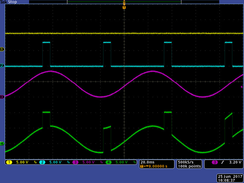
This image shows a +5V source, a unipolar 7.5V pulse, and unipolar 8V sine wave. You can see the addition of the three waveforms and the clamping (when the green trace flatlines) at +10V.