|
259 Complex Wave Generator Module |
|
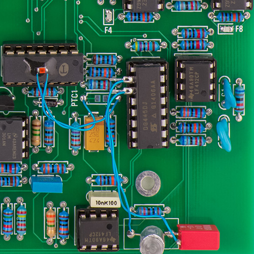
I built a 259 V1 Complex Wave Generator module for someone else. They sent me a complete kit of parts and I assembled and tested the module. Many of the components are sourced through Mouser but specialized parts, the panel, knobs, and PCBs have specific sourcing requirements.
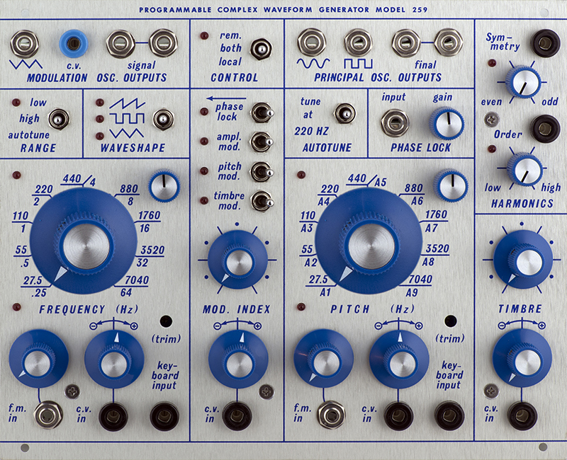
259 Complex Wave Generator description from the Buchla Synthesizer User Guide, November 16, 1981. This document doesn't describe the autotune switches which disable the FM input for tuning. I would be interested in what autotune is supposed to do. The clocks of IC11 and IC15 are connected to ground so these parts do nothing.
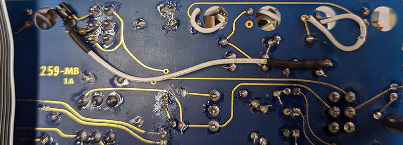
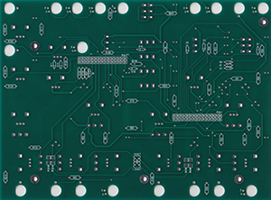
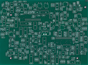
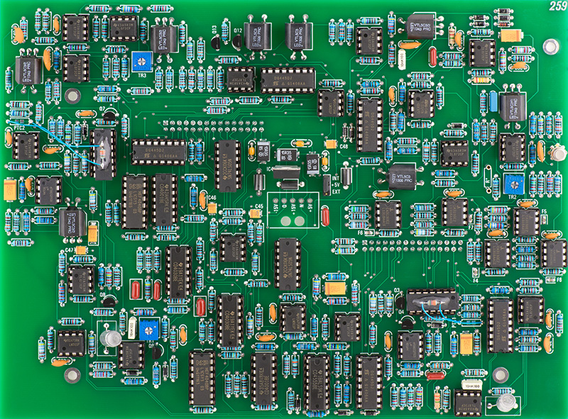
I made reference designators from the PCB images. The components cover the silk screen legends once populated which makes it hard to debug if anything is wrong.
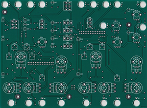
PCB 1 Front Reference Designators (includes trimmer identification)
PCB 1 Rear Reference Designators
PCB 2 Reference Designators (includes trimmer identification)
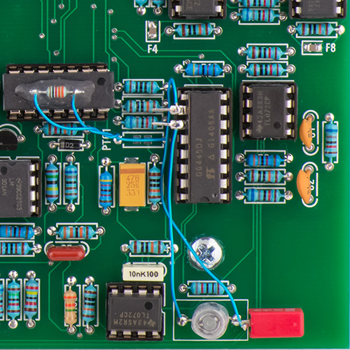
Construction
There is a single build thread and no modifications listed for the V1.0 PCB.
259 V1.0 Complex Wave Generator build tips
My Modifications and tips
Front Panel build
process
|
Build time for PCB1 and the panel was 3.75 hours. This is PCB1 ready for the final front panel installation (the image is a composite of two separate photos).

I use color coordinated wire for the banana jacks although there is only the single blue jack.
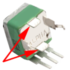
The tabs on the 9mm Alpha potentiometers contact the PCB so I cut the top and bottom tabs off of Pot4, Pot11 and Pot13 since there are runs directly beneath the tabs. I do not like relying on solder mask for insulation.
The square pins do not fully seat into the headers with the height of the standoffs. I insert the square pins fully into the female header and assemble the PCBs together. The pins are flush with the PCB and fully inserted into the header so the alignment is correct in all directions and then soldered in place.
Build time for PCB2 was 7.5 hours. The resistors take a long time to install since there are so many of them and they are spread all over the PCB. I use Kester .020" diameter #24-6337-6401 331 water soluble core solder so take time every hour to wash the PCB. The trimmers, vactrols, polystyrene capacitors, and power cable are added after washing. I epoxied the vactrols onto their respective transistor array and used SIP socket posts for R*.
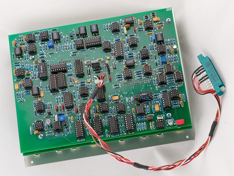
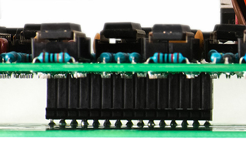
There are two 2x15 headers on the rear of the PCB.
Calibration
There are a number of calibration adjustments but the front panel trimmer nomenclature is misleading.
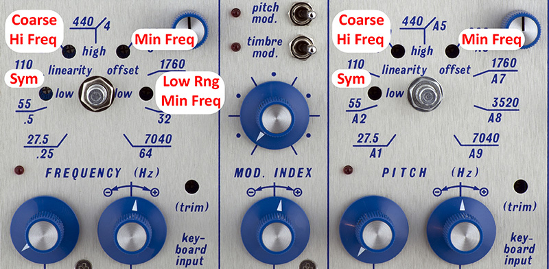
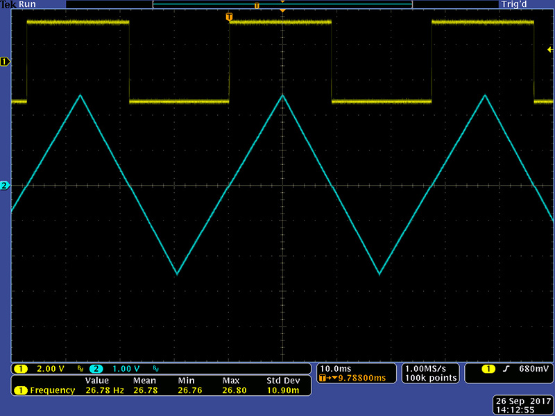
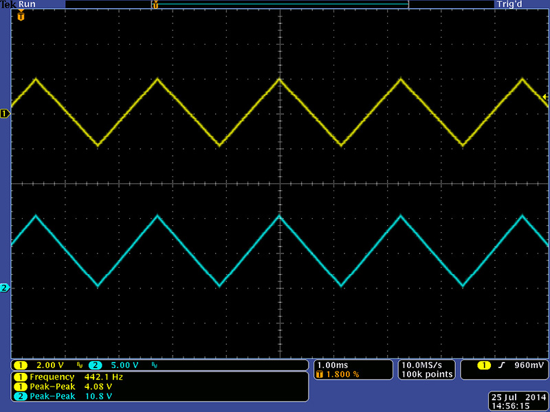
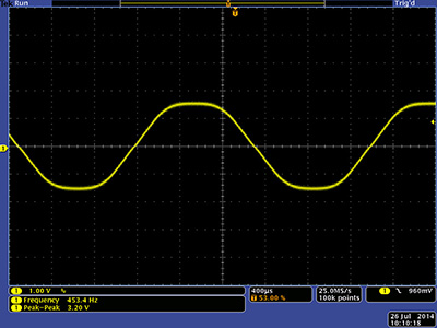
For either the MO or PO first adjust the symmetry at the lowest frequency (MO on high). The trimmer adjusts the current mirror so the rising and falling slopes of the core triangle are equal. Without this, at lower frequencies the period of the triangle will shift and the first octave or so will be out of tune. This image shows an out of symmetry principle oscillator. The rising slope of the triangle is controlled by the expo pair while the falling slope is controlled by the current mirror. Adjust the symmetry so the slopes are the same. The rising slope will not change so simply adjust the falling slope for symmetry. This photo is before adjustment.
Then set your trim to adjust the V/Oct. I typically monitor the square wave output as it usually provides more stable measurements. I usually chose a frequency around 50 Hz and then apply a CV 4 octaves up (4.8V for 1.2V/Oct. Then I check the accuracy at all the octaves (1.2V, 2.4V, 3.6V, and 4.8V for 1.2V/Oct) and iterate until I am satisfied..
Then center the fine control and set the coarse control to minimum and adjust the minimum frequency to 27.5 Hz.
Set the Coarse control to maximum and set the hi frequency to around 7 KHz.
For the MO set it to low and recheck the symmetry. Then set the low minimum frequency. Since it is so low in frequency I typically set the coarse control to midpoint and adjust for 4 Hz. Sometimes the MO low frequency waveforms can be quite distorted and I have Modifications below to address.
Operation
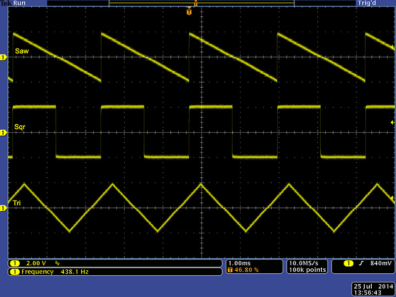
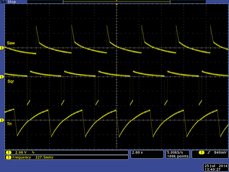
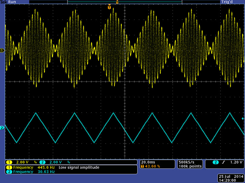
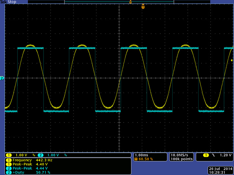
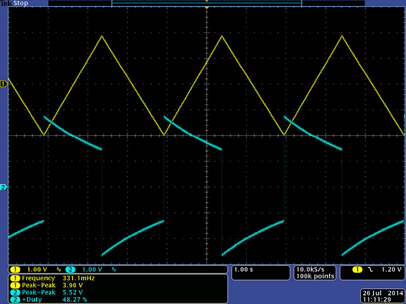
Calibration and full checkout of all inputs and outputs took about 2.5 hours. I calibrated the modulation oscillator at the center of the frequency control to 440 Hz (high) and 4 Hz (low). In high range the minimum frequency was 32 Hz and the maximum frequency was 8 KHz. The waveforms are well formed. This image is a composite of three scope images showing all three waveforms at frequency control mid setting.
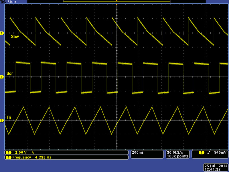
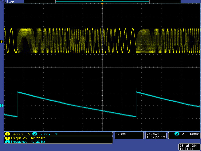
In low range the waveforms are a bit more distorted but generally pretty good. This image is a composite of three scope images showing all three waveforms at the frequency control mid setting.
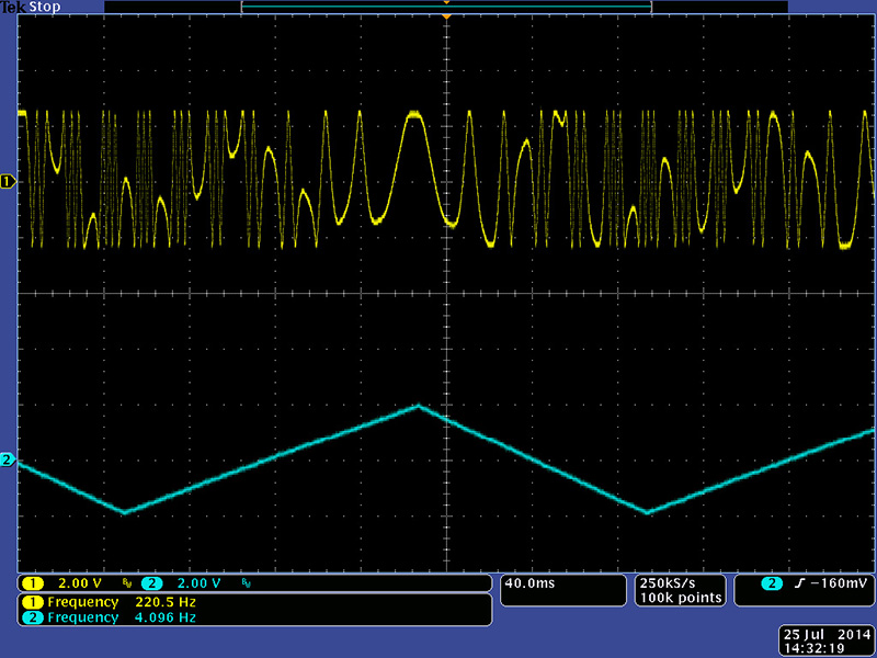
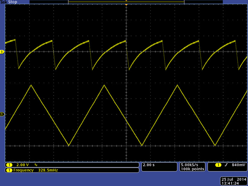
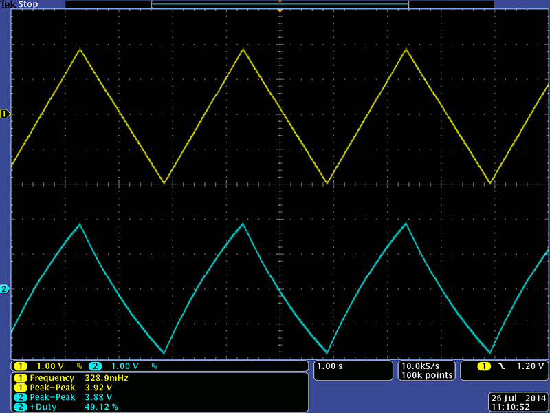
As you go to the very low frequencies the waveforms distort quite badly. At the low end of the frequency control the oscillation stops. This image is a composite of three scope images showing all three waveforms at the frequency control min setting. I made modifications to significantly improve the waveforms. Scope images of the improvement are in the Modifications section near the bottom of this page.
This image shows the difference in levels and offset between the modulation output and the CV output. The modulation output is a +/-2V output while the CV output is a 0 to 10V output.
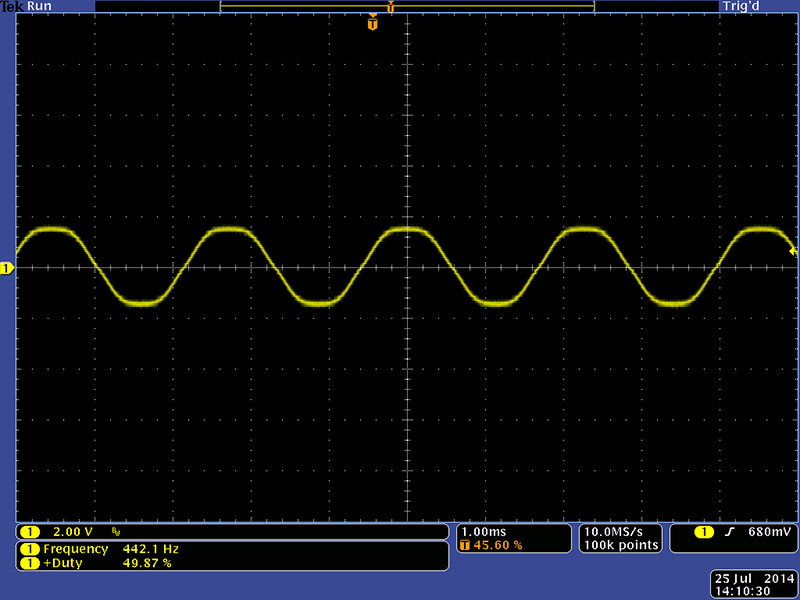
I calibrated the principle oscillator at the center of the frequency control to 440 Hz. The minimum frequency was 29 Hz and the maximum frequency was 9.8 KHz. The sine wave has a bit of flattening. I made modifications to improve the sine shape. Scope images of the improvement are in the Modifications section near the bottom of this page.
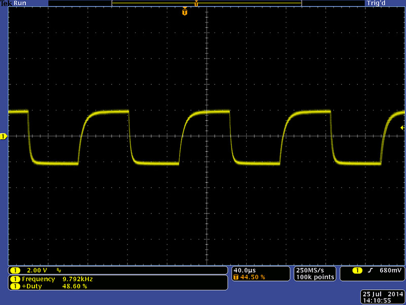
At the maximum frequency the square wave shows some leading edge rounding.
This image shows the amplitude modulation.
This image shows the frequency modulation.
This image shows the timbre modulation.
This image shows the principal oscillator with all modulation modes on (phase, amplitude, frequency, and timbre). It produces quite a complex waveform.
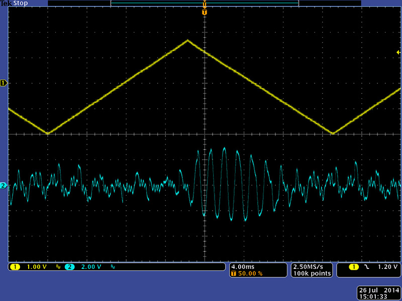
This video shows the principle oscillator phase lock capability to an external oscillator.
Modifications
I did some modifications to improve the flatted top of the sine wave (left image). I changed R110 to 787R (1K paralleled with R110)which rounded the top nicely (right image). The sine trim TR1 adjusts the gain a bit more with this mod so I could adjust the sine amplitude to match the square amplitude. This is a much better sine wave.

This image shows the principal oscillator sine and square outputs.
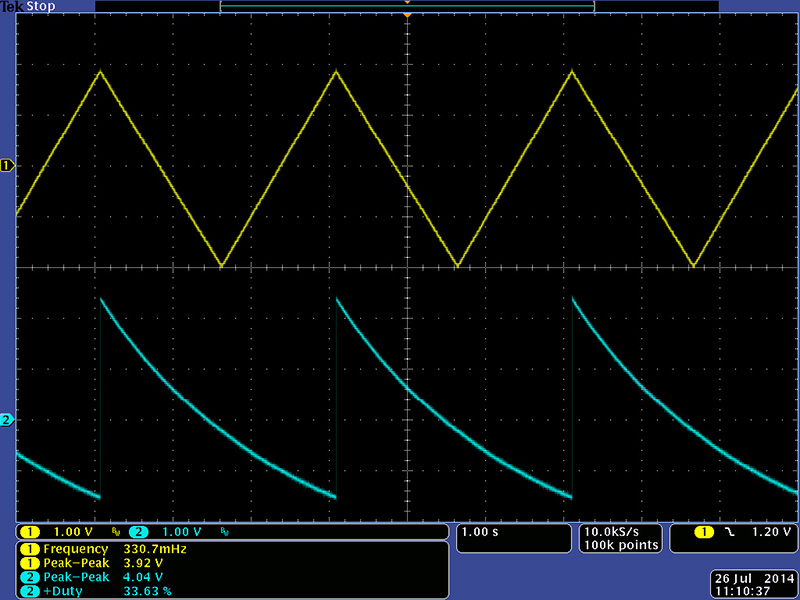
The modulation oscillator waveform distortion on the low range was quite significant. IC4C switches in a different bias point for the expo converter on low. I made some modifications to improve the match of the charge and discharge current sources but they negatively affected the waveforms on the high range. I decided instead to use IC4C to switch in a higher value integration capacitor which works very well. This image is a composite photo of the modulation oscillator lowest frequency before and after triangle wave (scope horizontal and vertical settings are different between the two and the top waveform is AC coupled). The resulting symmetry is very good..
Here are three scope images of the modulation oscillator output and the signal output at the lowest frequency of 1/3 Hz. The signal signal output is capacitively coupled so there is droop in the waveforms. However, all are much improved with a near perfect duty cycle.
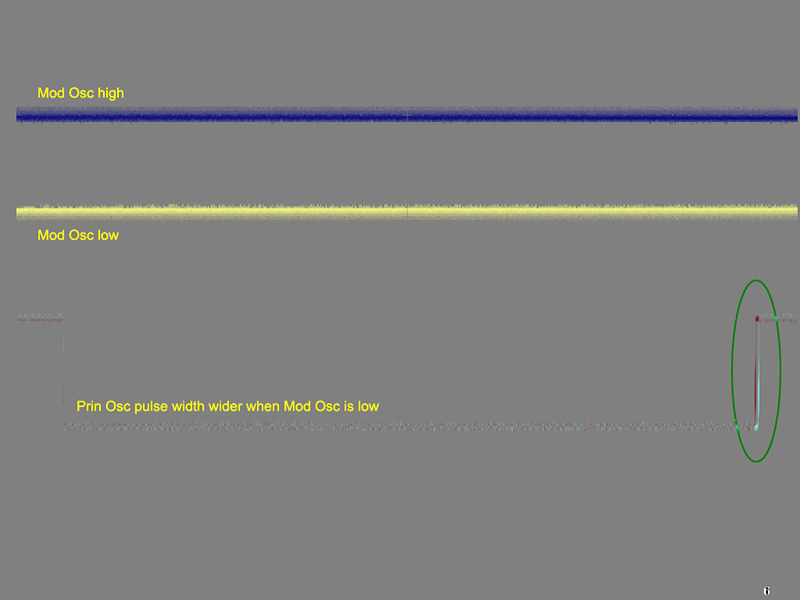
The forums mention a "bleed" of the modulation oscillator in the principle oscillator with all the modulation switches off. This module had a slight "bleed" that I could hear it as a timbre change in the square wave output. I could not hear it in the sine wave or final output. I investigated the principle oscillator circuit and found that the square output would vary in width depending on whether the modulation oscillator output was high or low. I took a scope image of the principle oscillator output with the modulation output high and inverted and added it to an image with the modulation oscillator low so similar colors become gray and unique colors stand out. You can see the difference in width circled in green and is about a 100 µS delta.
I decoupling some of the logic ICs (IC6, IC8, IC9, IC10 and IC11) in the modulation oscillator with a 0.1 µF capacitor across the IC power pins. This helped minimize the "bleed" so it was barely perceptible but I could still see some pulse modulation on the scope.
I investigated further and found the +15V shifting about 20mV depending on the polarity of the modulation oscillator output. This shift is independent whether the +5V is internal or external. This module appears to be very sensitive to +15V variations so I changed to a dedicated power supply with short cables and could no longer discern any "bleed". My recommendation is to make sure you have a well regulated power supply with short cabling for this module. I didn't analyze the power distribution on the PCB but suspect some modifications in the distribution and isolation of power routing would certainly improve performance.
Additional Builds and Modifications
This customer supplied SMT tempcos which I also epoxied to Q1 and Q5 and wired them to the PCB.
I took some time to further investigate the bleed between the oscillators. The architecture is such that the AM modulation is always enabled but the wet path is broken with an analog switch when turned off. I surmised that perhaps there was still AM modulation that might be impacting the power supplies that was causing the bleed. I looked at moving the analog switch from the wet signal path to the modulation index path but on this build I could not see or hear any bleed between the oscillators with all the modulation switches turned off. This build used LF412 op-amps which are not my favorite, no additional decoupling capacitors, and a Power One HDBB-105W-A with a 12" power cable and the +5 jumper set to external. The HDBB-105W-A is a large supply with 1.5A of +/-15V and 12A of +5V so it is well regulated and this seems to confirm my earlier experience that well regulated supplies are the key to minimizing bleed.
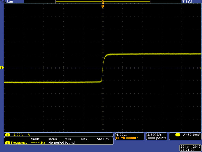
This Principle Oscillator square output showed some oscillations on the rising edge. You can barely see them in this scope image outlined in red.
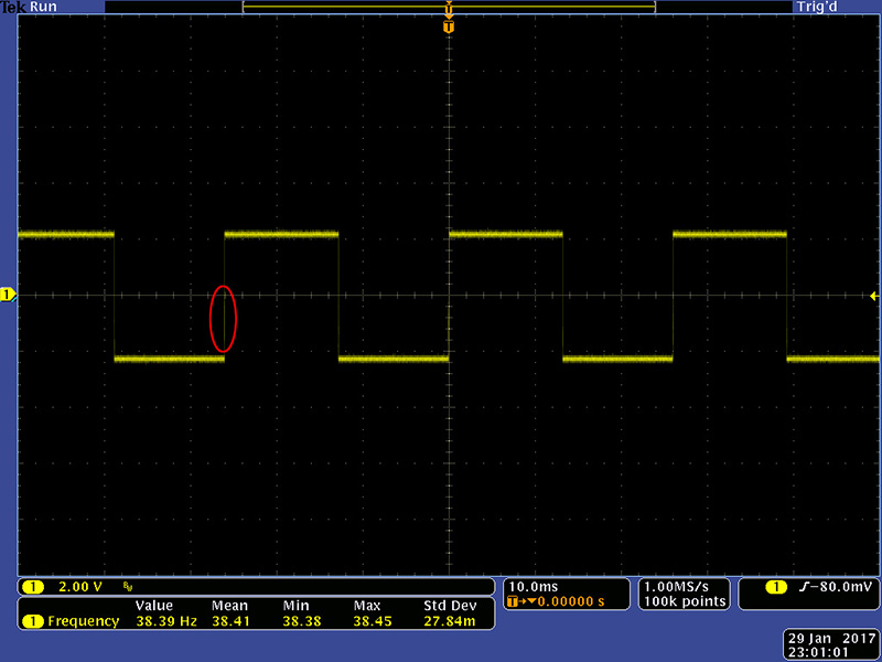
Increasing the sweep speed to look at the rising edge shows the oscillations.

U25 is a comparator to generate the square wave output from the triangle. It has no hysteresis which is simply bad design practice for a comparator. I lifted the triangle input, pin 2, and added a 10K series resistor. The other end of the 10K can connect to the anode of D9. Then I added a 1M feedback resistor from pin 7 to pin 2. The resulting square wave output is now clean.
Yet More Modifications
I have had to make a number of tweaks to various 259s that come to me for repair.
Sometimes I need to lower R107 (R149 vintage version) to dial in a nice sine shape. I have gone as low as 6K8.
Sometimes I need to lower R217 (R278 vintage version) to dial in the AM modulation. I have gone as low as 6K8.
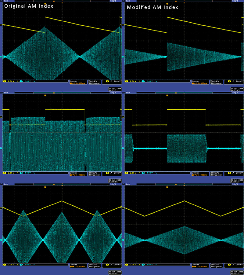
The AM Index way over modulates the signal. The "dry" signal is subtracted from a 100% AM modulated "wet" signal to generate the AM modulation. A vactrol-based VCO controls the amount of "wet" signal. The variation in vactrol performance will basically ensure that it is never correct. On many, 100% modulation occurs as early as a quarter turn. After this, the "wet" signal simply increases in amplitude thus generating a large distorted signal. I have adjusted R229 (R290A vintage version), sometimes with two series resistors, to dial in 100% AM modulation at full CW rotation. Values I have used are 1K, 910R+62R, 2K4+330R. This composite scope image shows the Final output with original resistor values on the left and modified on the right. These scope images show how over modulated the final output is where the ramp actually creates a triangle-shaped modulation and the triangle doubles the MO modulation.
Both V1 and the vintage version contain parts used for the auto-tune circuit that isn't fully implemented. There is a CD4040 counter IC in both oscillators (MO is IC11, PO is IC15) which are powered by 15V. The ICs driving the CD4040 and the ICs that the CD4040 drives are powered by the 5V reference (not +5V). As such the CD4040 output voltage is limited by the clamp diodes in the CD4030 which just burns excess current. I don't own a 259 so I have never experimented with just removing the auto-tune parts that do nothing. I simply lifted pin 12 and added a 49K9 series resistor to limit the current on both parts. In addition, pin 11 of the CD4040 is reset and is driven by parts operating on 5V. For 15V, Vil is < 4V and Vih is > 11V which isn't being met with a 5 volt part. The CD4040 reset is in the high state is in the undetermined voltage which can also increase power dissipation. Fortunately the reset input is always low.
V2 Vintage Version
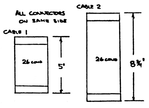
V2 reverts to copies of the original two PCB design. This image from the original reference diagram details the interconnect cable dimensions.
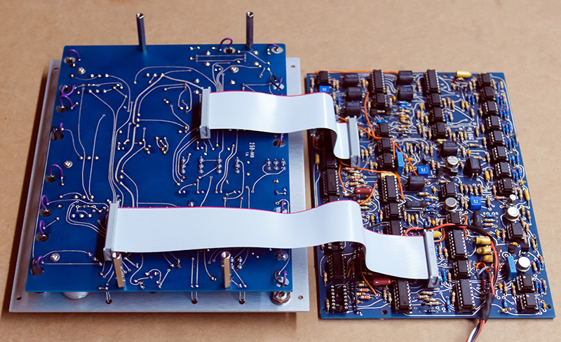
This photo shows the interconnect cables which allow the PCBs to lay flat for debug.
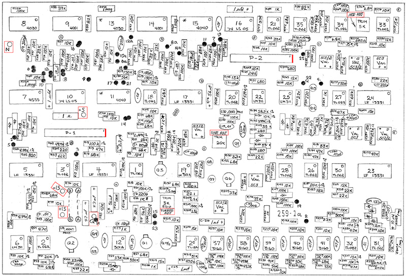
This portion of the reference diagram shows the locations of the three trimmers, the power supply connections, and the pin 1 (red stripe) designator for the cables.
This board takes an incredible amount of time to build since it is difficult to locate the actual resistor pads. I'd recommend the SAModular version which is silk screened. I have both JFETs in sockets as I want to select parts. I'll solder them in afterwards. I've epoxied the tempcos on top of the exponential pairs.

This design uses 1K tempcos R22 and R122, both marked with stars. R122 is associated with exponential pair Q5 and R22 is associated with exponential pair Q1. These tempco resistors compensate for the thermal component inherent in the exponential pair transistors. For best thermal performance the tempco and expo pair should be at the exact same temperature. It is common design practice to have them physically touch with some thermal grease between them but this vintage PCB layout simply has them in close proximity.
The principle oscillator square wave suffers from the same rising edge oscillations. You can cut the trace just above D7 and D8 and add a 10K resistor from these pads to IC25 pin 2 on the rear. Add a 1M resistor between IC25 pins 2 and 7 on the rear.
For 1.2V/Oct I use 82K resistors for R5A and R109A. TR1 and TR2 are 100K trimmers but that makes these trimmers very sensitive. I use 20K.
To correct the AM modulation I typically use a resistor around 1K for R290A. I select it so the AM modulation is about the same level and make sure I can trim the modulation to 100%.
Some people have reported either the MO oscillator stopping at the lowest frequencies or significant distortion of the waveform. At the low end the integrator core is operating on very low currents so cleanliness of the board is critical. Some have found improvements after washing the board several times. With sockets, flux can wick up around the pins and be trapped under the socket where it is hard to remove. I suggested the capacitor modification as described above which worked to their satisfaction in resolving the issues.
|
259 Vintage PCB Low Range MO modification.
|
These PCBs take a long time to build due to the number of parts and their random distribution. I made a parts locator for PCB2 with all of the part numbers and a grid location on the PCB. This hasn't been fully verified so let me know of any issues you find.
259 vintage PCB2 parts location updated 3/11/21
Epilog
I found one layout error on the PCB which doesn't really affect much. When the switch is set to remote, both oscillators should no longer be controlled by the coarse knob. The PO is, for a time. Mine was still operative for 15 seconds. IC17 is a DG445 which disables the coarse CV. Pin 12 is the logic reference voltage which needs to be +5V. This is connected to the control pin 9. As such, when you turn on remote, the reference and the input are both 0V. It must drift around for a while and then finally turn off. Cut the trace on the back of the PCB to IC17 pin 12. It connects to the d and e pads. Instead, wire pin 12 to +5V. I simply cut the trace and wired it over to IC4 pin 12. IC23 and 24 have the same issue. For IC23 you have to bridge the trace going to and from pin 12 after cutting both.
This note is on the bottom of page 2 schematics for the CO. It says you may delete these ICs for the non-digital mode. It is incorrect. IC13 is a CD4030 which is necessary as it controls the two CO LEDs. It needs to be installed.

There is a modification on Modwiggler to use the Both switch to reverse the saw to a ramp. They don't fully explain the end-result operation, but I believe while the mod does this, in Local mode the waveforms don't match the panel legends. I added a transistor to invert IC7 pin 14 when in Both. This leaves the wave shapes original and matching the panel when in Local, and in Both the saw is replaced by a ramp and the square is replaced by the triangle. The truth table below shows the wave shape modes.
| IC7 pin 14 | IC7 pin 13 | Function |
| 0 | 0 | Triangle |
| 0 | 0 | Ramp |
| 1 | 1 | Square |
| 1 | 1 | Saw |
When in Both, I force IC7 pin 14 to 0V which changes the selection from the saw to a ramp, and the square to a triangle (a more elaborate modification could have changed just the saw). I simply wired a 2N3904 transistor with the emitter to the local-both-remote switch, the base through a 10K resistor to the local-both-remote switch, and the collector through a 220K resistor over to one of the switching diodes. This photo shows the modification I made on a customer's 259 repair. Sorry about the poor cell phone quality.