|
289 Dual Defect Processor Module |
|
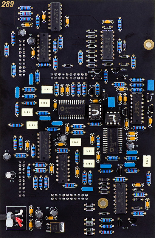
I built a 289 Dual Defect Processor module for someone else. They sent me a mostly complete kit of parts and I assembled and tested the module. The PCBs, eeproms, and panel are from the ElectricMusicStore and nearly all of the PCB components are sourced through Mouser.
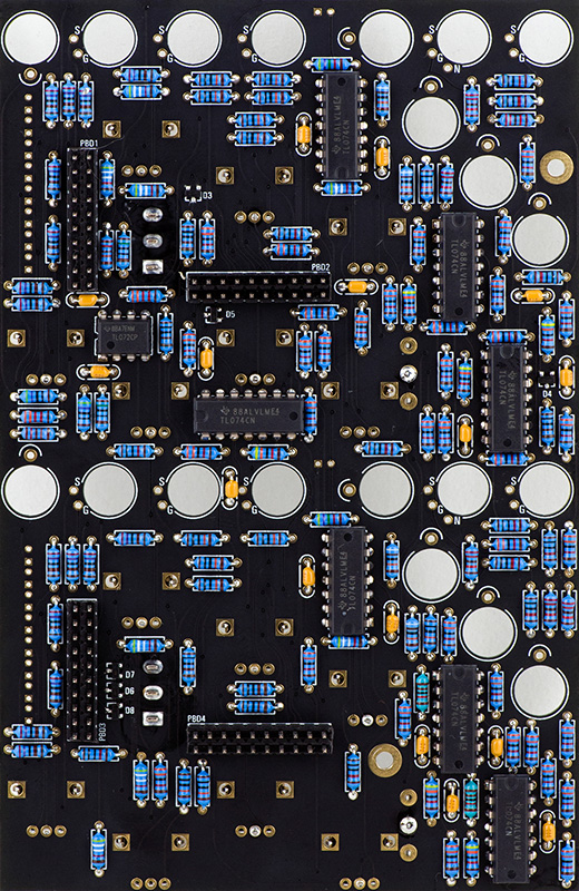
I made reference diagrams from raw PCB images.
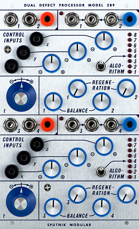
This is a very complex module and the jacks and controls are non-intuitive. The DIY version does not have the same patches as the pre-assembled version.
| Upper Patches | Lower Patches |
| 1. 2-Tap Proportional Delay 2. Harmonizer 3. Filtor 4. Phasering 5. Yuverb 6. Rail Resonator 7. Ampressor 8. Vocoder |
1. 4-Tap Rhythmic Delay 2. Psychorus 3. 8-Band Correlated Comb Filter 4. 3-Band Stereo Equalizer 5. Mirroverb 6. Hall Reverb 7. Samsara Wheel 8. Brainulator |
I've created a 2 page PDF with a description of the patches found on the web.
289 DIY Dual Defect Processor Patch Sheet
Construction
The 9mm potentiometers have tabs that touch the PCB. There are several positions on the PCB where there are runs underneath the tabs. I break the tabs away so they will not rub through the solder mask and short to the runs. I wish these PCB layouts would include clearance zones.
I always mount the male pins on PCB1 so that PCB2 has the female pins. PCB2 has the power cable and using female headers on the backside means nothing can short to them if PCB1 is not attached. I also solder the female headers first, insert the male pins, and mount the two boards together before soldering the male pins to PCB1. This elevates the male pins a bit off the PCB and ensures they are fully seated when assembled. This PCB uses BAT54S which Mouser no longer carries but they do carry the BAT54SFILMY (Mouser 511-BAT54SFILMY).
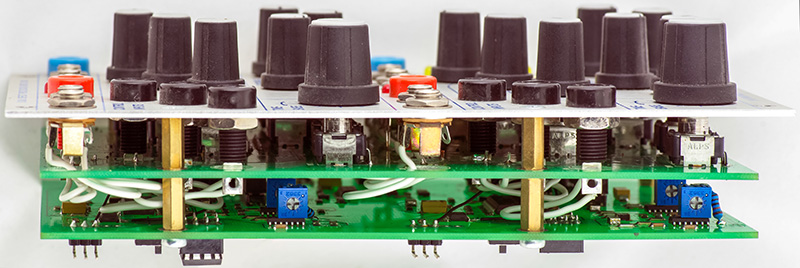
I also use the front panel to align the switches for soldering. I have the potentiometers mounted but not fully soldered. I always solder one pin, assemble the panel, and then on the 9mm potentiometers solder the remaining pins while centering the potentiometer. For the 16mm potentiometers I reflow the one pin to relieve any stress due to height and then solder all pins. You can see the unsoldered potentiometer pins in this photo.
PCB2 has the surface mount SPIN chips. I only used sockets for the eeproms. Two sets of three transistors are labeled A, B, and C which can sometimes indicate matched. You should buy these in cut tape but I matched them on my Tektronix 576 curve tracer.
Modifications
Although the BOM calls out 10K - 100K Lin for Pot1, Pot2, Pot6, and Pot7 you want to use 10K. These are part of the balance control and higher values affects this circuit. In fact I would use 10K Lin for all the 9mm potentiometers for better linearity. I also question the 100K Lin for Pot3 and Pot8 but have no technical information and cannot trace the runs with this black soldermask. It would be interesting to compare a 10K vs. 100K.
The Spin FV-1 input levels are a bit hot with standard signal levels so the overload light comes on often. The 289 EMCloned build thread indicates to lower R7, R8, R20, and R21 on PCB2 from 82K5 to 15K to attenuate the input signals. While this does attenuate the input to the Spin FV-1 by 2.5X it also attenuates the dry signal to the mix control. If instead you increase R13, R14, R15 and R16 on PCB2 you will only attenuate the input to the Spin FV-1. Increasing them from 100K to 200K attenuates the signal by 2X.
The Sum output jack is a unity mix of the two outputs. You can decrease R15 and R40 on PCB1 to lower the gain. 75K decreases the gain to 0.75X.
The Dry and Wet signals are not unity gain when set to CCW and CW. These changes are for 10K Lin controls for Pot1, Pot2, Pot6, and Pot7. To increase the Dry gain change R6, R8, R31, and R33 on PCB1 from 100K to 91K. Changing the Wet gain is a bit more complicated as the level varies with the Mode and the Regeneration controls. I found that decreasing R5, R7, R30 and R32 on PCB1 from 100K to 49K9 seemed reasonable. With some Modes and Regeneration you can drive the Wet into clipping.
Sputnik 289 Modifications
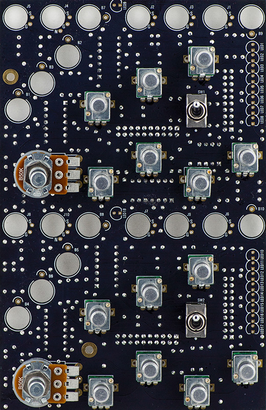
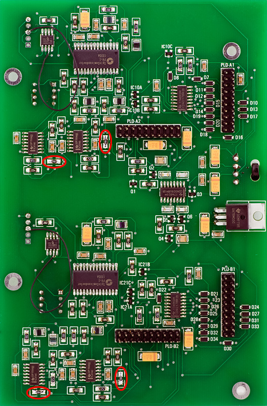
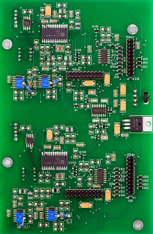
The same Spin FV-1 input attenuation modification can be performed on the Sputnik Modular 289. The rear PCB is all surface mount and the resistors are indicated on this image circled in red.
These four resistors are between the output pin 1 and the input pin 6 of the nearby ICs. Pin 5 is the positive input and is grounded. Since adding sockets for a thru-hole resistor is a challenge on a surface mount board, I decided to simply add 100K attenuators. 1/4" trimmers fit perfectly on top of the ICs and the end legs are the spacing between pins 1 and 5. I then added a 100K from the wiper to the pad that connects to pin 6 and this helps support the trimmer. I chose to not epoxy the trimmers to the ICs. There is sufficient solder on the IC legs to hold the trimmer firm.
This close-up of the trimmers shows how they are mounted. The end legs are folded down to connect to the IC pins.
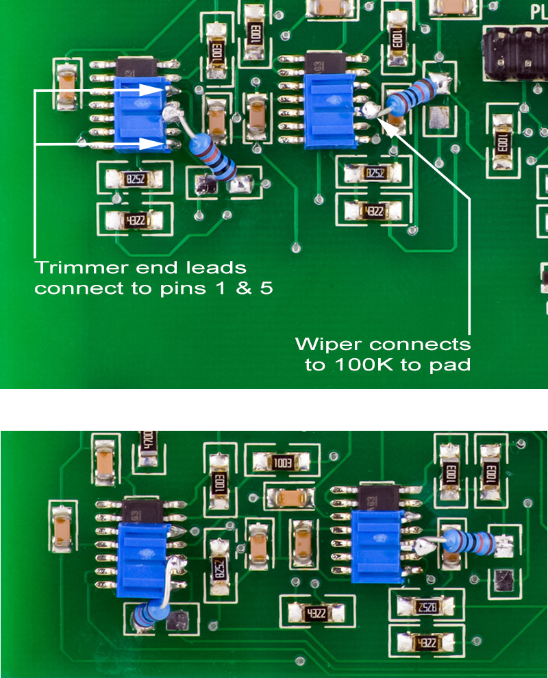
The trimmers can be easily accessed from the side.