 |
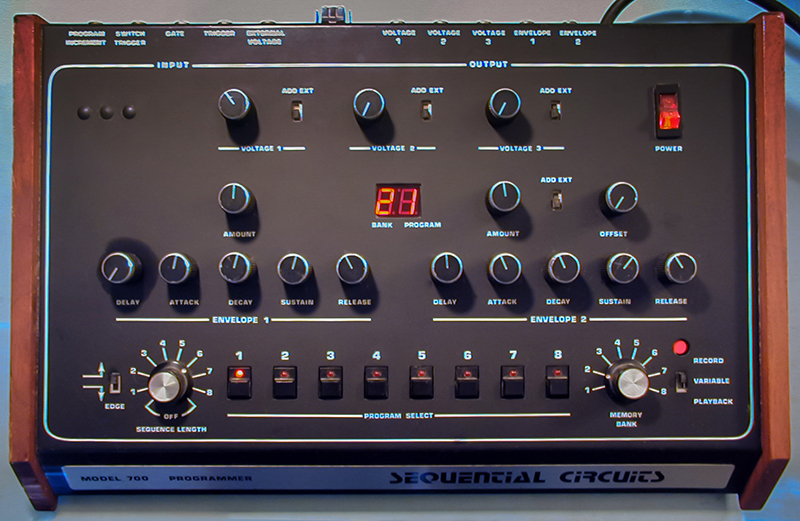
Sequential Circuits
Inc Model 700 |
|
I don't own a SCI Model 700 Programmer but was sent a 1977 serial number 0051 for repairs. This was the earliest version of the programmer which had no external trimmers and used CA3080 OTAs. I am documenting these vintage instruments since there is so little information available, and especially on the early version. There is a nice summary on restoring a later version Model 700 Programmer on the AMSynths site SCI Model 700 Programmer - Restoration & Cloning.
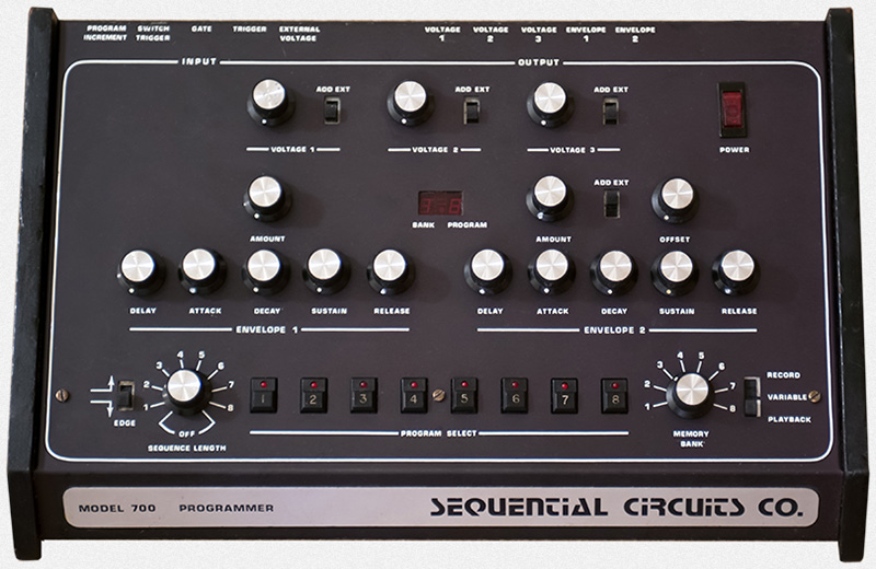
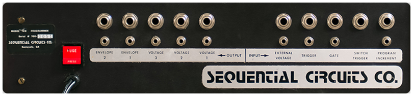
The rear panel is divided into inputs and output with both 1/4" jacks and 3.5mm jacks. I've connected with people who used to work at SCI looking for schematics and one told me of a useful modification that was sometimes made. The the two internal delay CVs could be brought out to additional normalled CV jacks on the rear. Plugging into the jack would disable the delay for a standard ADSR function and provide an additional CV out.
I can find no schematics for this OTA version but Riley Smith was kind enough to scan me a set of the Rev1 SSM-based schematics.
SCI Model 700 Programmer Rev1 Schematics (SSM based version)
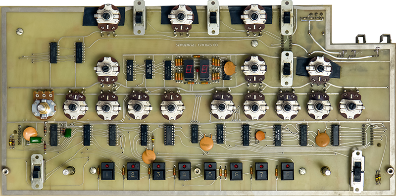
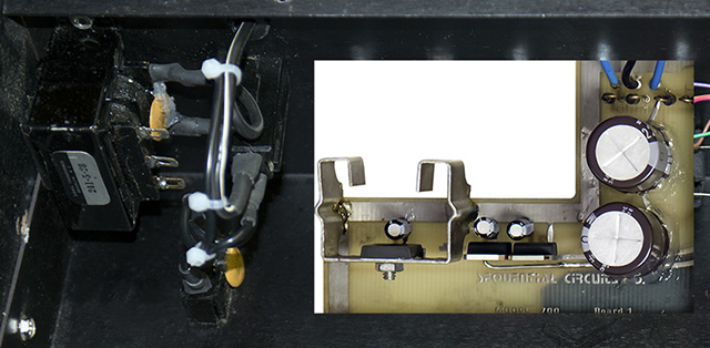
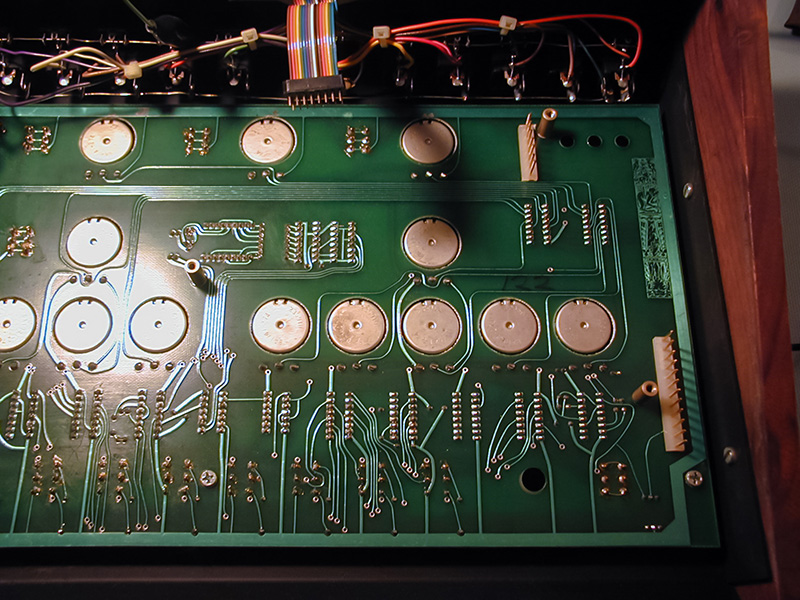
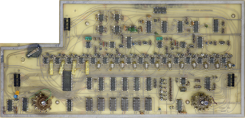
The top PCB is board 1 and contains the power supply components on the rear, LED display, controls, switches and the clock circuitry. Three 16 pin DIP headers connect it to board 2. Note the tape under the potentiometers to insulate the runs underneath.
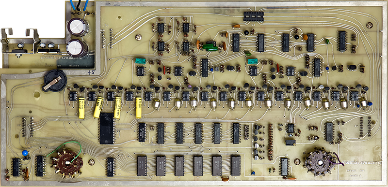
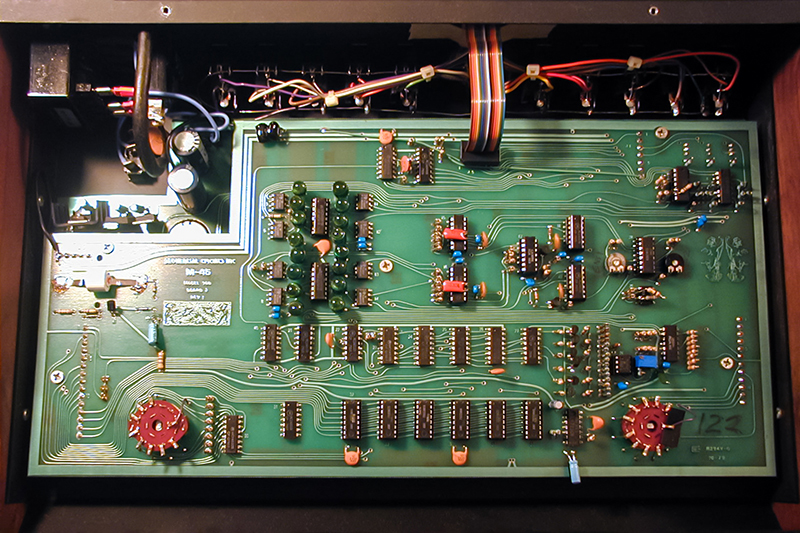
The bottom PCB is board 2 and contains the two rotary switches, sample & holds, ADC, DAC, and ADSRs. The 1Kx1 memories are the only parts in sockets. Originally there was an AA battery holder mounted near the transformer but it was missing so I added a lithium coin battery holder on the PCB. The blue and black wires connect to the power transformer.
Architecture
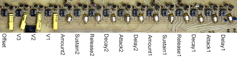
The design is a discrete logic (e.g. no microprocessor) architecture using 6 bit control words. Each of the 16 words in a program is a 6 bit value for a stored control - Voltage 1, 2, and 3, EG1 and EG2 Delay, Attack, Decay, Sustain, Release, and Amplitude, and EG2 Offset. There are 8 programs (8 x 16 = 128 words) in a bank and so the 8 banks (8 x 128 = 1024 words) fill the memory.
There are a number of low frequency clocks derived from a 50 KHz master clock that sequence all of the functions. A 4 bit counter is clocked by one of the low frequency clocks and is used as the address counter for the 16 control words in the selected program. The address counter also drives an analog input multiplexer for the 16 controls which go to a 6 bit ADC (analog to digital converter) which drives the RAM data inputs. Another set of multiplexers routes the RAM data inputs (variable mode) or the RAM data outputs (playback mode) to a 6 bit DAC which drives 16 sample & holds generating the 16 quantized outputs. The ADC consists of a simple ramp comparator driven by the high speed clock comparing the control multiplexer with the output of the DAC. Quite simple!
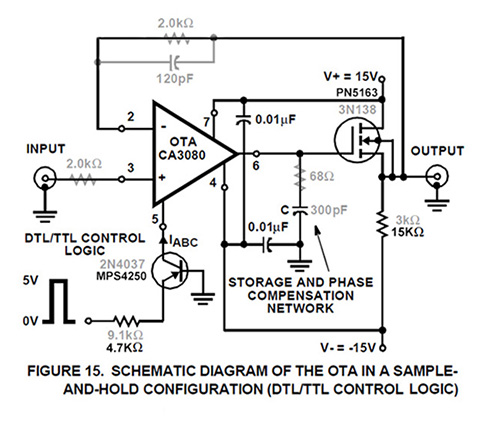
In the Rev1 version the sample & holds are implemented with 4051 demultiplexers driving capacitors with op-amps as voltage followers. In the first version 16 CA3080 OTA sample & holds and are sequentially strobed by a 4 line to 16 line decoder. The OTA sample & hold is is very similar to Figure 15 in the 2002 Intersil AN6668.2 CA3080 Application Note (Ap Note components and values are greyed out where different).
Repairs
There was a lot of physical repair required. There were many solder blobs, broken runs, and smashed parts with shorted leads. The boards were saturated with spray cleaner and there were blobs of glue randomly spread around the PCBs.
The power supply had been badly repaired, parts were shorting together and primary wiring was exposed. The +/-15V regulators had been moved off PCB with added heat sinks wrapped in tape. Oversized electrolytic capacitors interfered with the primary components and wiring. What a mess - the power supply had to be completely rebuilt.
Replacing the correct parts on the PCB and using heat shrink and RTV to insulate the primary wiring was the first repair.
One of the DIP PCB interconnect headers had a broken pin and someone had wired that connection between the two PCBs. I knew it would be difficult finding a new DIP header with the same physical height so I cut away the corner plastic, replaced the pin, and made a form for epoxy to rebuild the corner of the header.
Physical inspection identified one broken resistor, a couple of smashed transistors so the leads shorted together, and a couple of damaged runs. One of the PN5163 FETs had a lead broken off so I cut away part of the case, soldered a 30 gauge wire to the stub, and added epoxy to provide strength. Delay2 was inoperative so I traced out each of the sample & holds until I found the Delay2 section where there was another broken resistor.
This image shows the layout of the 16 sample & hold circuits.
One potentiometer had been replaced with a poor substitute so I replaced it with a Bourns 241 series (Mouser 652-PDB241GTR02104B0 on the far left in the board 1 picture) which was a perfect replacement except for solder lugs instead of pins. Another potentiometer was very stiff which was due by the front housing being misaligned with the rear cover.
The memory did not function but the controls still operated in playback mode so something was wrong with the switching circuit. An examination of that circuit found several open runs but no signs of any scratching or cutting - strange. It was almost as if the PCB was under-etched. Repairing those runs restored memory functionality. There was no battery holder for the memory so I added a lithium coin battery holder on the rear of board 2.
Program switch 5 would sometimes operate bank 6. The CD4051 multiplexer was especially sensitive to crosstalk between the address lines and the switch 6 input on pin 5 whenever switch 5 was pressed. My first thought was a bad multiplexer since I have seen these fail with internal cross-connections. The new the multiplexer corrected the problem but I could still see some crosstalk on the signal due the NC on switch 6 being intermittent so I added a 0.001 µF capacitor from pin 5 to to ground to clean it up. Bob Grieb sent me an email that he saw similar issues on a Model 700 that he was repairing and his solution was to add a 10K pulldown resistor on the multiplexer output pin 3. This solves the problem for any switch NC contacts that are intermittent.
And finally, of course, the fuse had been replaced with the wrong value. All of the repairs were mechanical in nature so this Programmer has seen some rough abuse and bad repair!
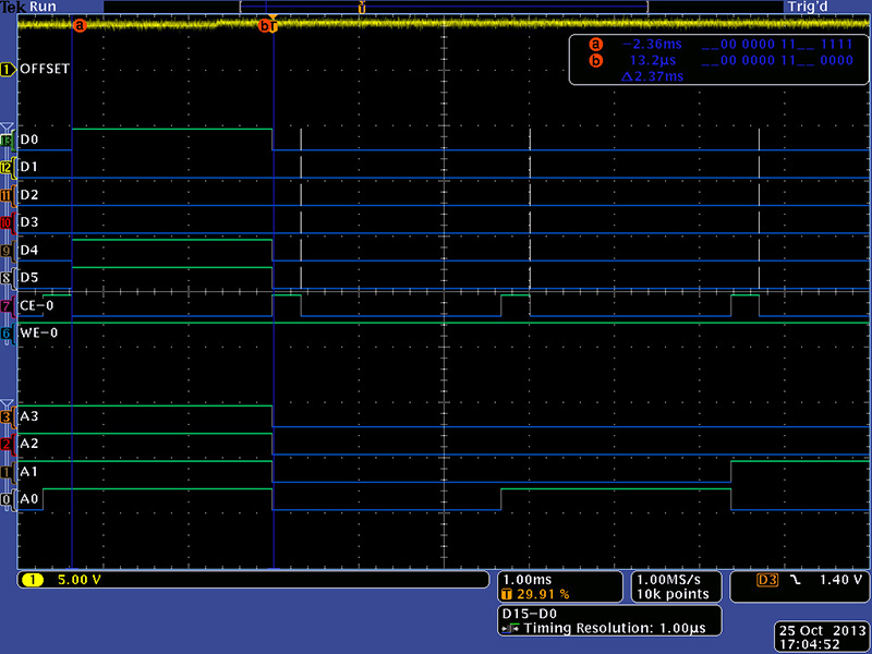
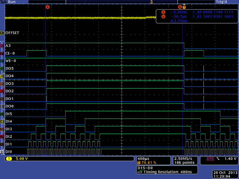
I needed to verify the memory was good and retained data during power cycles. I put a logic analyzer on the the memory and varied the Offset control until I found it at address XXFH. I set arbitrary input values and stored them in memory which I could verify with the logic analyzer before and after power cycling. This logic analyzer image shows an Offset value of 31H (D5 - D0 between cursors a and b).
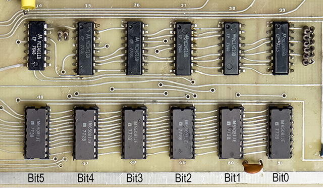
This image shows the layout of the memory.
I reconfigured the logic analyzer so I could monitor both the data input and the data output lines and triggered on the falling edge of A3 to view the Offset word value (prior to the falling edge).
This logic analyzer image shows the ramp A/D determining the value of the Offset control (DI5 - DI0). The data input lines are the output of a 6 bit counter that counts up and stops when the DAC value of the counter is greater than the Offset control value. The final counter value represents the ADC value for the offset control. The ADC clock is ~50 KHz so counting to 3DH takes 63 x 20 µS = 1.2 mS conversion time and the maximum value of the Offset control is 3DH. You can also see the data outputs all go high at the falling edge of CE-0 until they read the correct memory value.
Operation
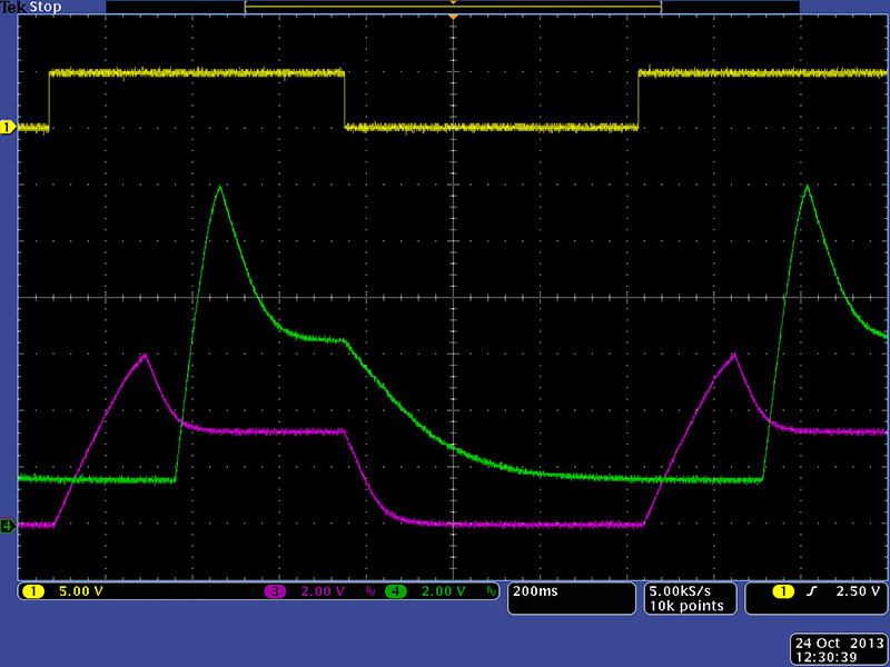
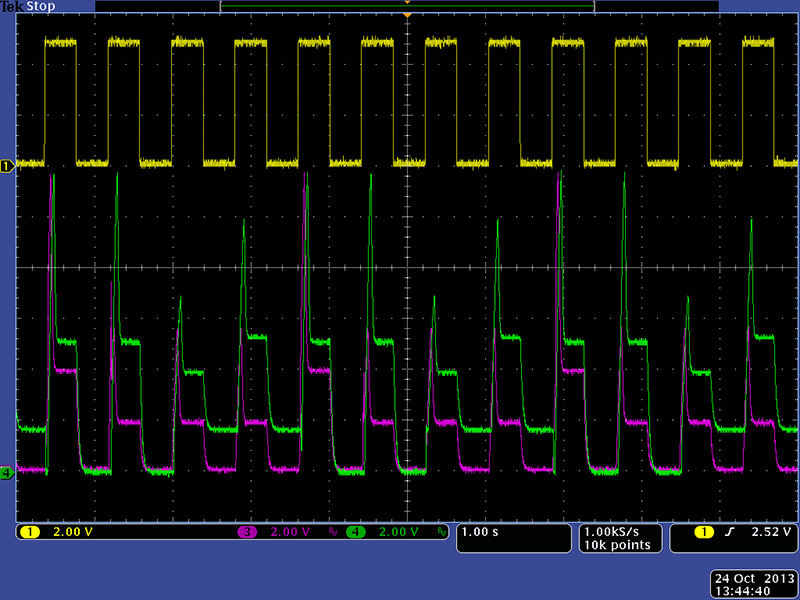
This image shows the two ADSR outputs driven from a Gate signal. ADSR2 is shown in green and you can see a different amount (amplitude), delay, and offset.
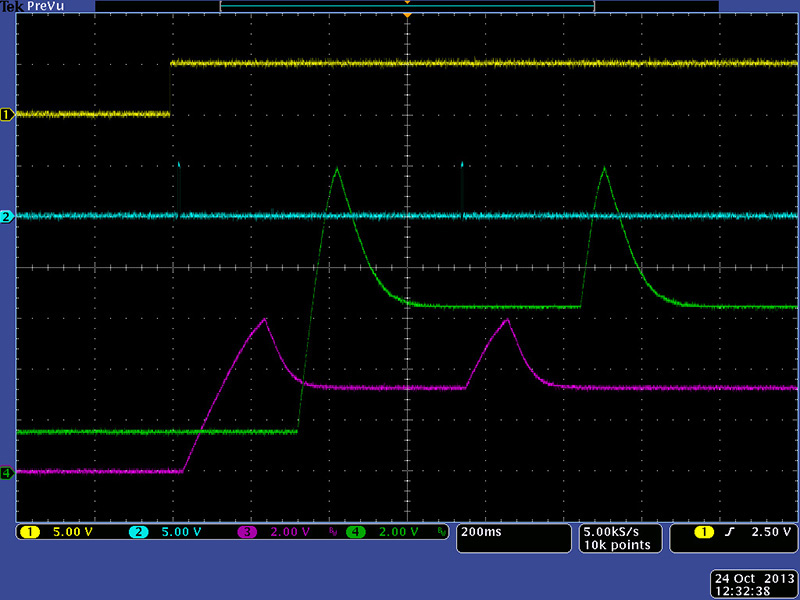
This image shows the same setup but using a Trigger. The envelopes do not start until the Trigger is received and a second Trigger restarts the sequence.
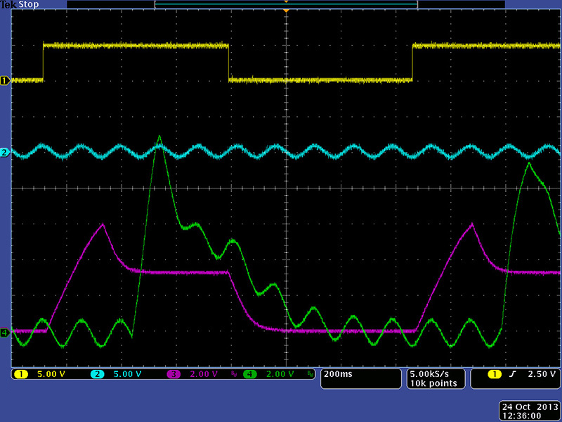
This image shows an external voltage modulating envelope 2 using the Add Ext function.
This final image shows a 4 step sequence of different stored ADSRs which differ by amplitude and offset.
Mk 2 Images
Bob Grieb was kind enough to send me some of the photos of a Mk2 Model 700 Programmer that he repaired. In this image you can see the three plugs in the upper left for the Voltage 1 - 3 scale adjustments and the different style knobs. The Record switch is now separate from the Variable / Playback switch
This photo is the rear of Board 1 and you can see design improvements. The board is solder masked, the potentiometers are aligned into holes in the PCB and there are no issues with interference with runs, and the board-to-board interconnect has been improved considerably by the use of single row pin headers. You can also see the three holes in the upper right right of the PCB for clearance to board 2 for the voltage scale adjustments.
Board 2 is completely redesigned and is quite different from the original.
Epilogue
This same SCI-700 came back to me for further repairs 2 years later for dead Envelope Generators. Since both were dead I assumed there was a common cause which proved to not be the case. It was very difficult following the circuit since there is no schematic. I did remove the PCB and photographed the front and rear and super-imposed them so I could follow most of the traces without having to keep removing the PCB as the interconnects are quite fragile.
I was able to trace out enough of the circuit to find a faulty 4136 op-amp that restored Envelope Generator 1. From the working one I was able to deduce the delay capacitors (blue) which generate a delayed gate with a CD4013. That switches the Attack voltage thru a CD4016 to a CA3080 OTA which charges the timing capacitor (red). A PNP transistor creates a pulse at the peak of the attack cycle which resets the CD4013 and switches the CD4016 to connect the Decay voltage to the CA3080 OTA input. The other input of the OTA is reduced in voltage so it then discharges the timing capacitor. The timing capacitor is buffered by a PN5163 JFET which was the fault on Envelope Generator 2. I replaced it with a J108 JFET.