|
5U Benjolin Module |
|
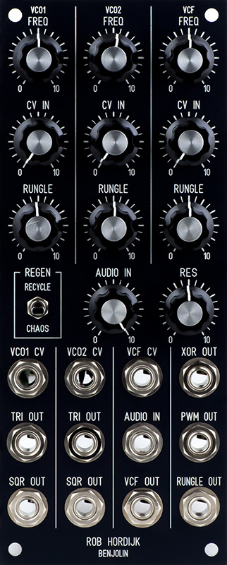
I built one of the first V0.2 PCBs for the Muffwiggler Benjolin module as described at Rob Hordijk Synths Info Website and also on the Muffwiggler thread Benjolin PCB? The Benjolin was designed by Rob Hordijk to be "bent by design". The Benjolin has four separate functional blocks consisting of two VCOs, one VCF, and a "Rungler". The rungler is an 8 bit shift register that is clocked by VCO2. The shift register data is the output of the shift register either direct (Recycle) or XOR'd with VCO1 (Chaos). The shift register output is fed to a 3 bit DAC (8 levels) which provides the Rungle CV fed back to the two VCOs and the VCF through the Rungle attenuators. This creates stepped voltage patterns of variable length and depth that give this module its characteristic sound. The input to the VCF is an external input with attenuator, a pulse width modulated signal derived from a comparator fed by the two triangle VCO outputs, and the rungle CV.
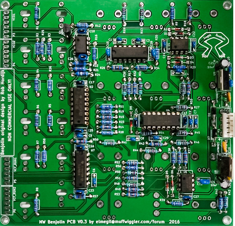
The controls and jacks mount on the front of the PCB along with a handful of resistors. The PCB is 4.90" wide by 4.95" high.

Most components mount on the PCB rear.
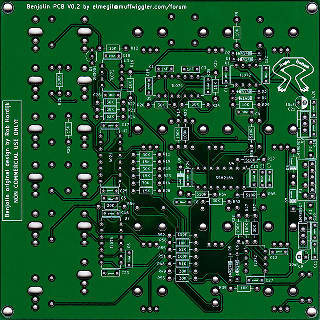
The BOM is available in the thread but I made modifications by adding sockets, changing to Xicon resistors, selecting in-stock parts, a standard length toggle switch, and Kobiconn jacks so all parts except the V2164 could be purchased from Mouser. The Kobiconn connectors require wiring the ground lug to the PCB and are a bit shorter.
Benjolin Mouser BOM (updated 7-11-2016)
The IC pin 1 markings are easy to miss. The silk screen at one end of the IC has a small "L" in the shape to indicate pin 1 as shown in this image.
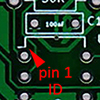
I made reference diagrams from the PCB images and colored pin 1 on the ICs red.
Construction
The CD4021 is operated on +/-9V, so a total supply of 18V. However, these regulators are +/-4.4% so the supply could be as high as 18.8V. Some CD4021s, such as the TI, are specified for a maximum voltage of 20V so there is some margin. However, other parts, like Fairchild, are specified or a maximum voltage of 18V so there is a possibility of over voltage. Make sure you use a 20V part for U2. Mouser carries only the TI part.
The first four hand modifications are required:
V0.2 Modifications
Optional Modifications
|
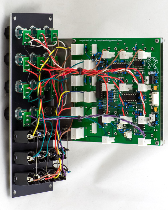
The PCB has headers for either a MOTM power or Dotcom power connector. The MOTM connector holes are too small for the MTA connector. I modified the MOTM pins using a small file on the corners to round them where they fit through the PCB. A 5 pin 0.100" MTA with two pins removed can be slightly bent to fit the 3 pin jack pads. This image shows the Benjolin assembled PCB after my addition of the XOR double buffer. All connectors are on the front side.
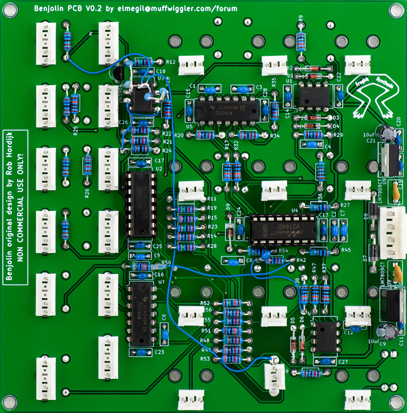
Many of the resistors on the rear of the PCB could have been mounted on the front but I matched them with their silk screen. The series output resistors for XOR, PWM, VCO1 Sqr and VCO2 Sqr have not been inserted pending verification of the output levels.

Operation
My rungler would not operate with a 2N3904 transistor without decreasing R25 considerably. At 10K it began to operate and at 1K it operated quite well. That 2N3904 had a measured beta of 175 I replaced it with a BC550C which had a measured beta ~700 and it operated with R25=100K. However, the resulting level did not meet the CD4021B specifications for levels. I added a double op-amp to boost the signals and then discovered the silk screen for the transistor on the PCB is rotated 180° for a 2N3904 so I had both transistors installed backwards. That no doubt was the source of my issue. I rotated the BC550C transistor and had good signal levels.
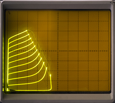
As an aside note on transistors operating backwards, the left image is a curve tracer image of a BC550 transistor with a beta of ~720. The right image is a curve tracer image at the same settings with the BC550 transistor backwards. The curves are quite scrunched indicating a much lower beta and a much lower reverse breakdown voltage. Note the long persistence of the phosphor which still faintly shows the previous image.
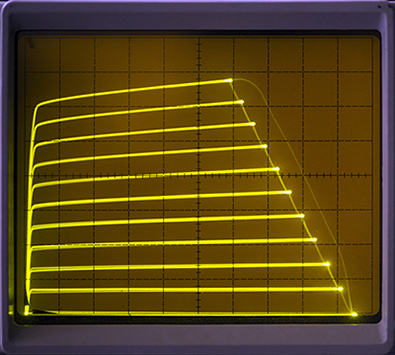

I adjusted the settings on the curve tracer for the backwards BC550 and it indicates a beta of 20. Given that the rungler operated, although with lower signal levels, there might be issues using a 2N3904 which has a minimum beta specification of 40.
The TI CD4021B does not have a specification for VIL and VIH operating at 18V. VIH is at 70% of Vdd at 5V and 10V operation and at 73% at 15V operation. If you assume 73% then VIH would be 13.14V at 18V operation, and shifted down by 9V would be 4.14V. VIL is at 30% of Vdd at 5V and 10V operation and at 27% of 15V operation. If you assume 27% then VIL would be 4.80V at 18V operation, and shifted down by 9V would be -4.20V. Thus the logic input to the CD4021B needs to be <-4.20V or >+4.14V.
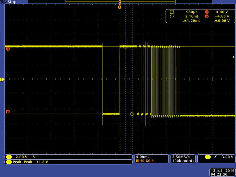
This scope image shows the XOR output and VOH measures 4.40V and VOL measures -4.6V. These are both within the assumed specifications for the CD4021 but with margins of only 0.2V VOH and 0.4V VOL. Note that there are different output levels depending on the logic levels of the two inputs.
Before I realized my BC550C transistor was in backwards, I added a TL072 dual op-amp piggyback on U3 with a gain of -3 followed by a gain of -1. This clips the XOR signal rail-to-rail to a constant output level and meets CD4021B input levels with margin. 1K6 and 2K5 series resistors drop the XOR Out to +/-5V. Since I already built this circuit I will leave it on the PCB since it improves the margins for the CD4021B. It also has the advantage of providing a uniform XOR signal level.
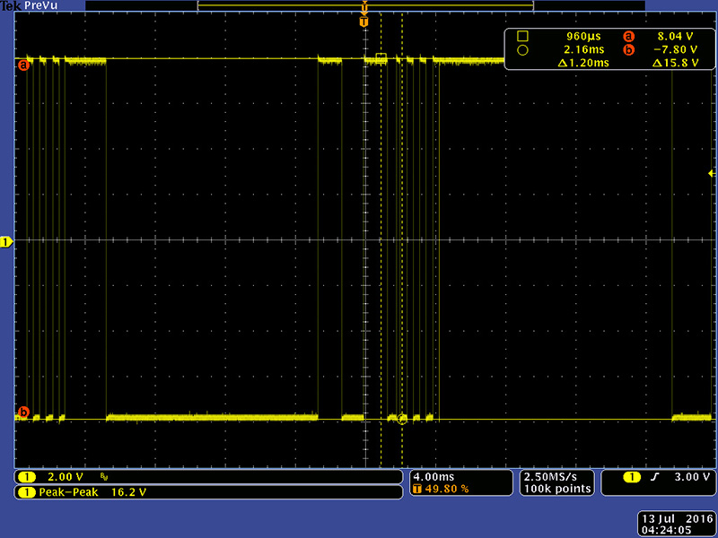
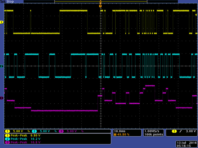
This scope image is of the two VCO outputs at +/-5 volts pk-pk.
This scope image is the same VCO settings with some rungle modulation.
This scope image is the same VCO settings showing Rungle Out and +/-5V pk-pk XOR and PWM.
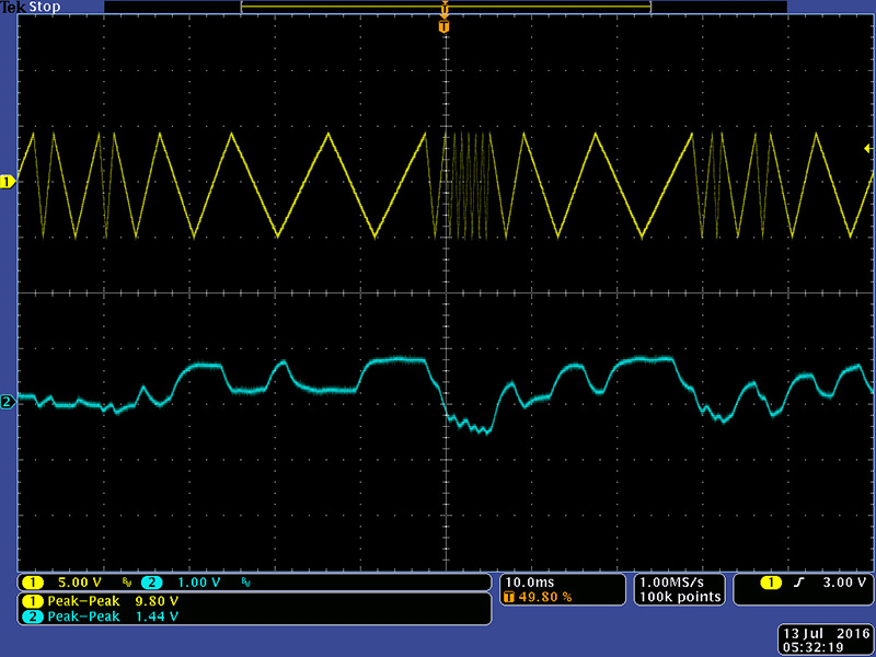
This scope image shows the low level filter output with no audio input since the PWM and Rungle CV is mixed into the input. The top trace is VCO2 before attenuation by the Audio In control. I later removed R51 so these signals are not fed to the filter input.
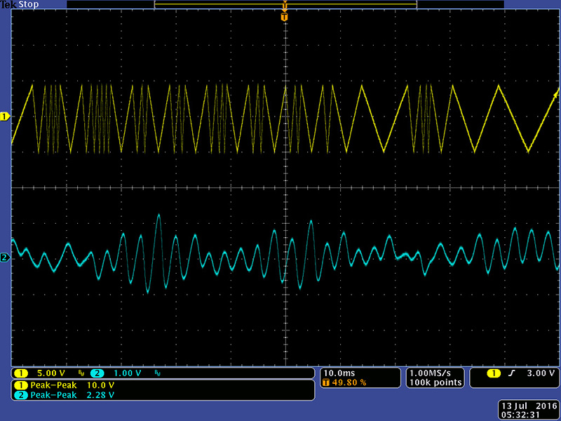
This scope image shows adding some resonance to the filter with no audio input. The signal level nearly doubles.
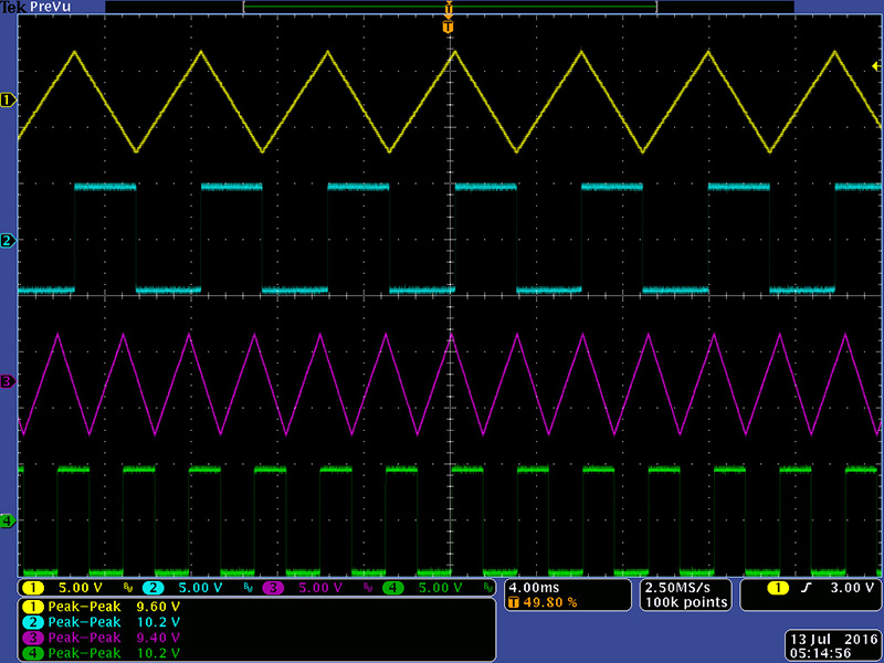
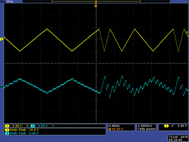
This scope image shows VCO2 now input to the filter with some modest filtering. The output level is 4V pk-pk.
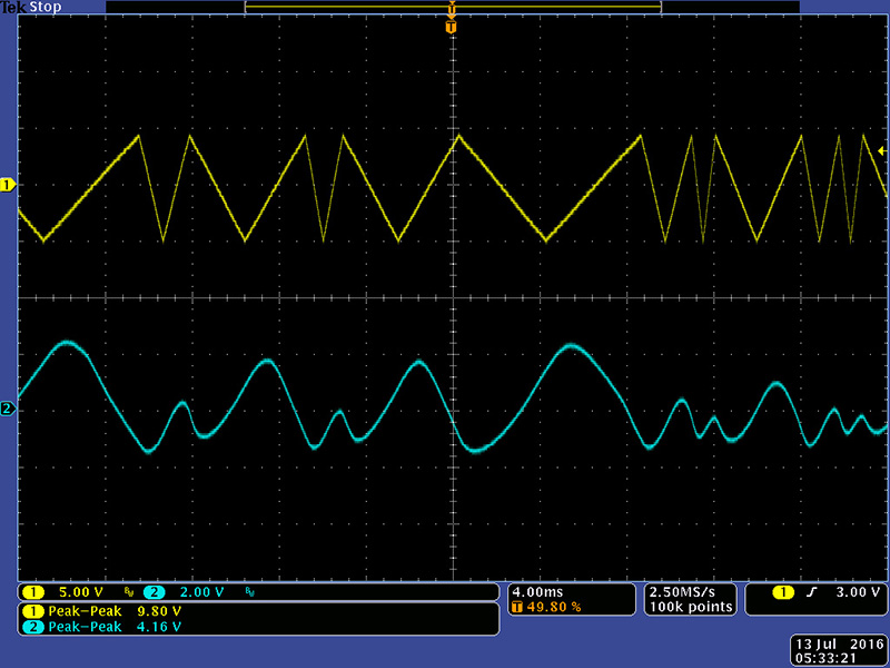
This scope image shows the same settings with some resonance added. The level doubles to 9.4V pk-pk.
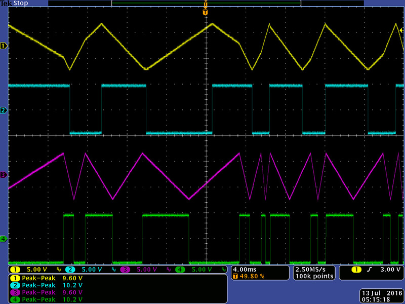
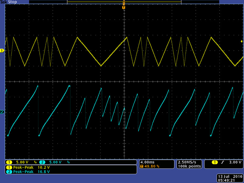
This scope images shows the maximum output I could get by adjusting resonance to maximum. Some of the peaks are clipping at 16.8V pk-pk which is the maximum headroom when operating at +/-9V.
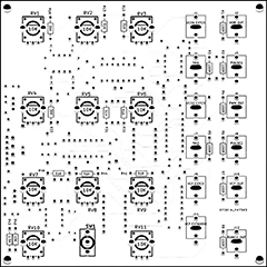
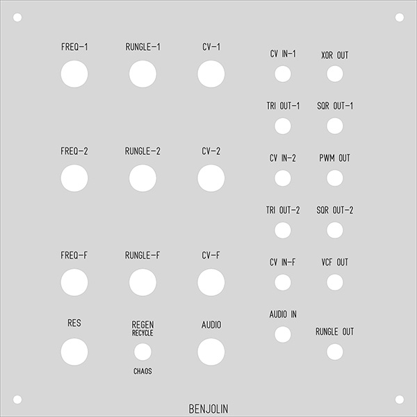
Panel
I designed a 2U MOTM-style panel using the Alps 9mm RK09L 10K potentiometers. The bushings are a bit short for a 3mm panel so I milled 16mm diameter cavities 1mm in on the rear of the panel. The 1mm cavity turned out to be a bit too deep so I used two internal-tooth lock washers on the rear. I could not use a potentiometer for a bracket so I used one jack and a rear stud for mounting.
After I fabricated the panel I modified the switch to a 3 position (as described above) so the nomenclature doesn't exactly match.
DJB 2U Benjolin Frontpanelexpress design file
There are a total of 60 wires connecting the switch, 11 potentiometers, and 12 jacks. However, there are only 25 signals as follows:
Common ground to jacks and potentiometers. (1 wire)
Three frequency controls and -9V. (4 wires)
3 CV inputs and Audio In jacks wire to the potentiometers. (4 wires)
Rungle potentiometers and rungle (4 wires)
Output jacks (8 wires)
Resonance (2 wires)
Switch (2 wires)
I used chicklets to solder to the Alps 9mm potentiometers. You can barely see the rear stud under the top row of potentiometers closest to the bracket. Wiring was difficult to bundle since it is so spread out across the PCB.
V0.3 Update
This is an image of the V0.3 revision of the PCB where the front panel control signals have also been brought out to 1x6 headers to make it easier to hand wire the module in a different format.
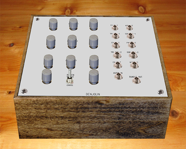
Tabletop Stand-Alone Design
I did not build a tabletop stand-alone box but did design a basic 6" x 6" panel design. The potentiometers and jacks are on a 1" and 3/4" grid. My calculations indicate that the jacks and potentiometers sit about 0.050" below the height of the switch. The easiest way to accommodate this is to use 0.050" thick internal-tooth washers on the jacks and potentiometers. The Kobiconn jacks are another 0.020" shorter so it would be easiest to mount them on the panel and solder them 0.020" off the PCB.
6x6 Benjolin Frontpanelexpress design file unverified
A tabletop version would fit nicely into a square wooden box similar to my Circle Machine.
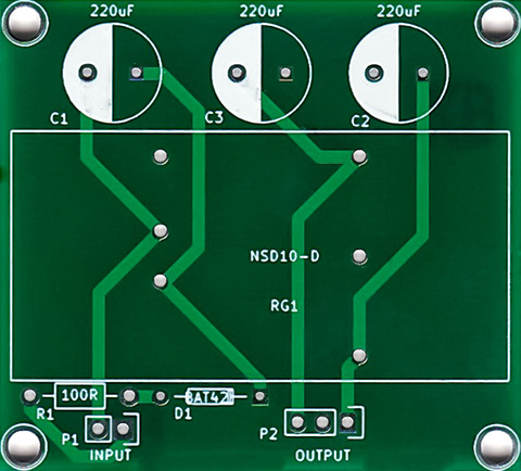
The DC power PCB for standalone operation uses a Meanwell NSD10-12D12 which requires a 12V DC input and has +/-12V outputs up to 420 mA with a minimum load requirement of 20 mA. The PCB has input polarity protection and additional filtering.