 |
DJB-PSIM / CVS Expansion Project |
|
This is an expansion PCB which will provide sixteen additional 8 bit ADC inputs and 16 additional digital inputs or outputs for the PSIM or ComputerVoltageSource module. The design uses inexpensive I2C components and requires only +5 volts and a two wire interface. There are two daisy-chained MOTM-style power connectors and a voltage regulator to generate the +5 volts. Two 2 pin MTA style connectors will interface directly to J3 and J5 on the PSIM or to the External I/O connector on the ComputerVoltageSource module for I2C signals and power.
During debug I managed to take out my AtomPro28 and MCP23008 (ouch!) with a voltage glitch. I had not bothered to put over and under voltage protection on the I2C interface. I have since modified my CVS with 51R series resistors and schottky clamp diodes to +5 and ground. I added these changes to the board design (and also my CVS) although I will not be ordering more boards to verify the modifications. I believe the problem was due to running multiple power supplies and feeding over voltage to the I2C inputs while one board was powered up and the other powered down. Since the power consumption is so low, the best solution is probably to run this board from the PSIM power supply on connector J5.
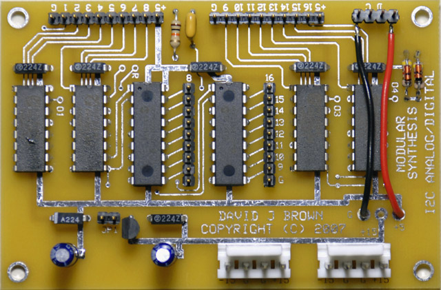
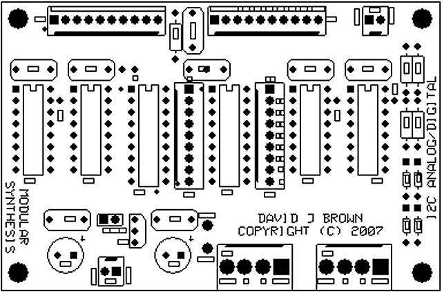
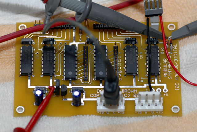
This PCB was designed for the ExpressPCB mini-board service which provides three quick prototypes for $51 without silk screen or solder mask. The design incorporates ample spacing so that solder mask is not required and all nomenclature is implemented in the top metal layer. The top photo is my prototype which is powered by a 4 wire cable from my CVS module. The lower layout is the revised PCB with the additional I2C protection components and the +5 power connector moved.
Expansion Design Files
DJB
Analog/Digital ExpressPCB design files (Unbuilt
/ not verified) ![]()
16 Digital I/O Configuration
I built a version of the board with just the two MCP23008 for a 16 digital I/O configuration. I am using it with some jumper clips to simulate switch closures to ground.
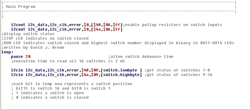
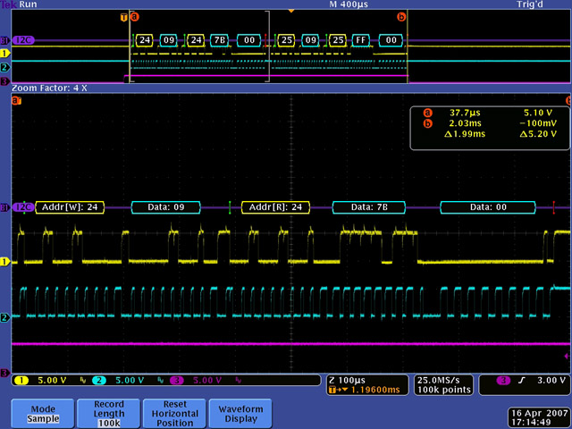
This demo program scans and displays switch closure information. The I2C commands to read all 16 switches takes 2 mS to execute (note - this code was written for BMIDE and changes are required for Studio).
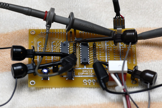
The I2C data transfer can be seen in this scope image. The $7B byte indicates switches 3 and 8 are closed. I have no idea what the extra $00 byte transfer is after the data byte. I have seen this before with AtomPro I2CIN commands and the byte seems to be ignored.
I2C switch demo.DJB.bas
This program is a demonstration of the 16 digital input channels. The
PCB is configured with 16 input switches. Any switch closure is indicated
by the run LED and the binary number of the switch-1 is displayed in the output
LEDs. For example, closing switch 4 would display the output LEDs
"off" "off" "on" "on" representing
binary 3. The highest switch closed is displayed.
16 Channel Analog Inputs
I built a full version of the board and tested the MCP23008 portion with the I2C switch demo.DJB.bas program. I am powering this module from my CVS module so there is only one power supply. Current draw for the full configuration is < 5mA.
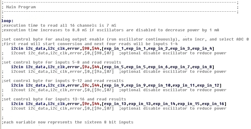
This demo program inputs all 16 analog channels and outputs the sum of each group of four inputs to the PSIM output (note - this code was written for BMIDE and changes are required for Studio). The I2C commands to read four analog inputs takes 1.75 mS to execute. All 16 channels can be read in 7 mS.
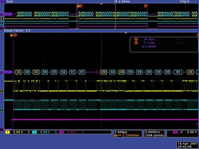
The I2C data transfer can be seen in this scope image. The first $00 byte is the result of the previous A/D cycle. The next four bytes are the results for inputs 1 - 4. Sometimes I will see an extra $00 transfer after the last byte as in the $4D sequence of inputs 5-8.
I2C ADC demo.DJB.bas
This program is a demonstration of the 16 analog input channels. Channels
1-4 are summed and output to the PSIM OUT-1, channels 5-8 are summed and output
to the PSIM OUT-2, channels 9-12 are summed and output to the PSIM OUT-3, and
channels 13-16 are summed and output to the PSIM OUT-4. Each input channel
represents 2.5 volts for a maximum of 10 volts on each of the outputs.
PSIM Expansion Programs
PSIM super sequencer
(rev0.5).DJB.bas
This is a modification of my CVS SuperSequencer (rev0.8).DJB.bas program for use with the PSIM with 16 expansion controls. It
also requires the LCD Support
module for the user interface. The program implements a 1 to 16 step programmable sequencer. Outputs consist of
CV, Trigger, Gate1, Gate2, and MIDI. Features include:
Programmable number of steps
Programmable Gate1 level per step
Programmable Gate2 level per step
5 mS Trigger
Programmable MIDI Program Change patch per step
Forward / backward step pre-tuning
Ordered and random sequencing
CV and MIDI output
The display indicates the Step number, Midi patch, Note number, and Gate1 and Gate2 levels
