|
258M-A Dual
Oscillator |
|
This MEMS 258MA is a faithful recreation of the 258A Dual Oscillator with a panel PCB for easier DIY construction. This oscillator differ from the later 258C in that the FM is an AC-coupled exponential input.

To make construction easier, MEMS has designed a front panel PCB for wiring of all the panel components. This much simplifies the DIY construction vs. hand wiring all of the components as on my earlier 258C build. This PCB can be configured for both the 258A or 258C and has additional trimmers for better calibration.
The 258A features two CV inputs with +/- CV controls. CV1 also has a fine adjust +/- CV control. As designed, scaling is done for the CV2 input with full CW rotation of the input control. CV1 is not scaled and requires operation of the fine adjust CV control along with full CW rotation of the input control for correct scaling. 1.2V/Oct scaling requires four resistor changes which are included in the build instructions. Located on the PCB are also two 20T trimmers which allow for precise CV1 and CV2 scaling. An additional trimmer sets the maximum frequency of the coarse control.
This panel PCB is also setup for a switching Tinijax so that with no plug inserted, the outputs are cross coupled to the FM inputs. You can ignore the switched connection and just use a non-switching Tinijax if this feature is not desired.

The main PCB is an authentic reproduction of the 258A which uses an µA726 heated exponential converter. MEMS supplies a SMT adapter PCB which replicates the µA726. The adapter mounts using wires to the µA726 footprint. This photo is the main PCB before the µA726 adapter and ICs have been installed.

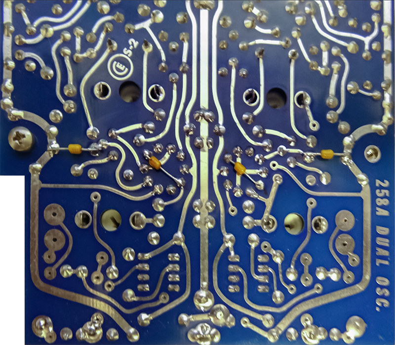
This photo shows the assembled panel PCB.

This photo shows the assembled main PCB

This photo shows the rear of the assembled module. The panel PCB trimmers can be accessed from the sides and bottom. The main PCB trimmers can be accessed from the rear.

Calibration
Calibration consists of setting the µA726 Replacer operating temperature, scaling the oscillators to 1.2V/Oct, setting the low frequency offset, setting the maximum coarse control frequency, and adjusting the sine shape and waveshape controls.
The 258A circuitry is a bit different from most other oscillators in that neither of the base connections on the expo pair are connected to ground. Pin 6 is used as a ground so R22 on the main PCB is replaced with a 0R or wire.

Information and calibration for the µA726 Replacer is on a this page.
These are the various trimmers on the panel PCB for calibration.

Note the panel PCB logo reflecting their new arrangement with Buchla.

These are the standard trimmers for the main PCB calibration.

Scaling Adjustment
The standard way to scale a 258 is to turn the CV2 attenuator to full clockwise and adjust the scale trimmer. CV1 is not calibrated and has the fine attenuator control to match CV2. The panel PCB has additional trimmers for CV1 and CV2 so you can do more precise scaling.
The BOM is setup for 1.2V/Oct scaling with the four 115K resistors on the panel PCB. These need to be changed if a different scaling is desired.
The main PCB scale trimmer is in series with the panel trimmers and scales both CV1 and CV2. I chose to center all four panel PCB scale trimmers and adjust the main PCB scale trimmers to get close. Set the CV2 attenuverter control to full CW and scale it precisely with the panel trimmer. Set the CV1 attenuverter control to full CW. You have to decide what to do with the CV1 fine control. I centered it so I could slightly detune CV1 +/-. Scale CV1 precisely with the panel trimmer. The design is quite accurate for 4 octaves and goes a bit flat on the 5th octave as there is no trimmer for high frequency compensation. I use my VCO Scaler for easy calibration (I donated this design to MEMS who made me a PCB).
Offset Adjustment
One of the idiosyncrasies of this design is with no termination on the CV inputs, the CV attenuverters will slightly vary the frequency. I calibrate the offset with the fine frequency control centered and both CV attenuverters centered. Turn the frequency control full CCW and adjust the offset trimmer for 5 Hz.

Coarse Control Range
The maximum frequency is typically beyond 20 KHz (this module was about 23 KHz). Turn the frequency control full CW and adjust the panel trimmer to set the maximum frequency at 20 KHz.

Sine Adjustment
The 258A has no symmetry trimmer and symmetry may not be ideal at the minimum and maximum frequencies. I adjust my sine shape at ~ 440 Hz. Adjust the sine trimmer for best shape. Depending on your JFET a resistor tweak of R60 may be required.

Waveshape Adjustment
Adjust the waveshape trimmer for best ramp and square. Depending on your JFET a resistor tweak of R43 and/or R46 may be required. The waveshapes are reasonable up to about 10 KHz.
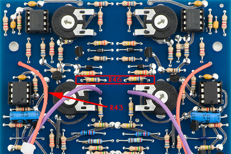


Above 10 KHz the waveshapes begin to degrade.


Epilog
An individual contacted me with an issue they were having with their 258A build. At a certain rotation of the coarse control, the frequency would jump and the sine would distort. I asked them to check the voltages around the expo converter and they found oscillations on the emitters when the change occurred.
I had them install a 1 nF capacitor from the R18 trimmer wiper to ground which is the offset voltage adjustment to the base of the expo converter to stabilize the reference voltage. This capacitor is added in the B version so Don must have found an issue. I also had them install a 1 nF capacitor across R21 which stabilizes the base voltage of the expo current source. That eliminated the oscillations and resulted in expected operation. They sent me this image of their modifications on the rear of the PCB.