|
296M
Programmable |
|
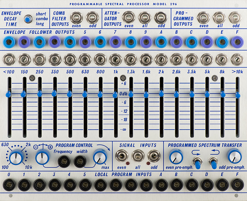
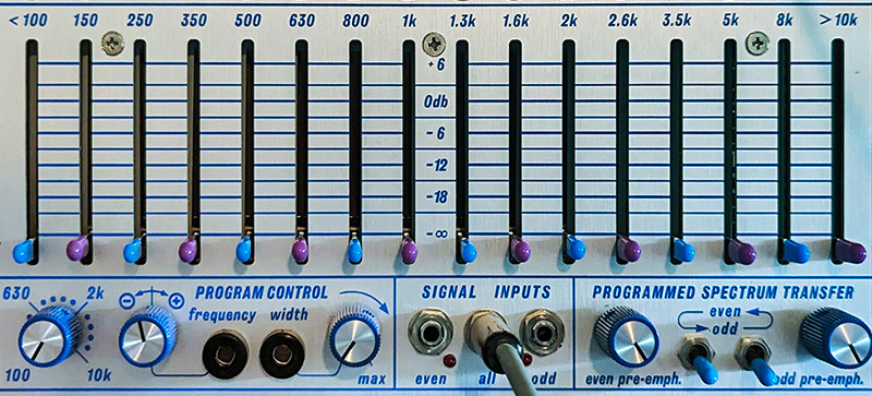
This 296 Programmable Spectral Processor is a complex design featuring 16 filters, envelope follower, programmed outputs using VCAs and special CVs generated from frequency and width controls, and transfer switches to map odd (or even) envelope follower CVs to the even (or odd) VCAs. It's best to read the manual to understand this module.
296 Programmable Spectral Processor Manual Transcribed from Buchla Synthesizer User Guide 11-16-1981
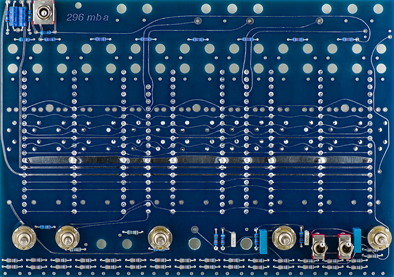
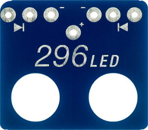
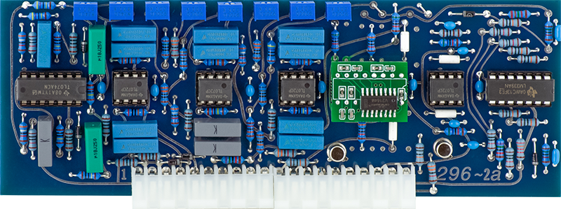
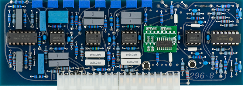
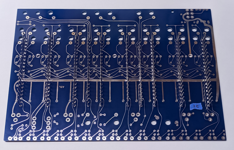
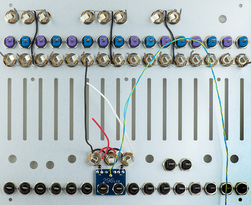
This 296 Programmable Spectral Processor follows the original through-hole layout. The motherboard does not yet have the sliders installed. The LEDs are the two sets of pads in the upper right.
These resistors mount on the rear since they are beneath the sliders. You need to solder these on the back/component side and cut the leads off flush with the front. The Alps slider insulators need to fit nearly flush with the PCB so you don't want a solder bump on the rear.
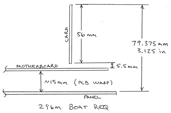
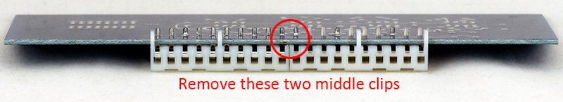
Note I have plastic headers on my Molex connectors. This increases the vertical space and this module will not fit in a 3" deep boat. Please see the construction section at the bottom.
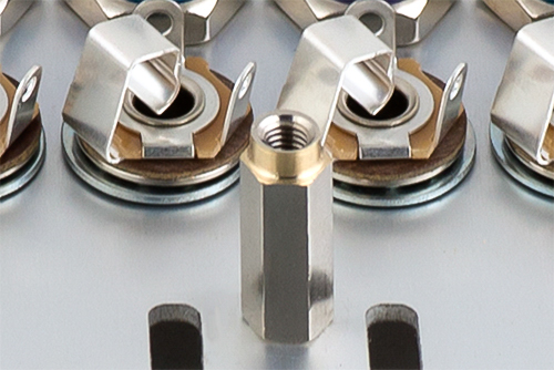
There is minimal clearance around the three standoff mounting holes in the motherboard so I turned the standoffs to ensure adequate clearance.
The LEDs do not have pads for mounting on the early PCB sets so need to be fastened to the front panel. I used epoxy and 30 AWG wire to run to the PCB pads in the upper corner.
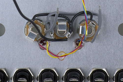
They now have a LED PCB which mounts on the two banana jacks with a second nut to mount the LEDs.
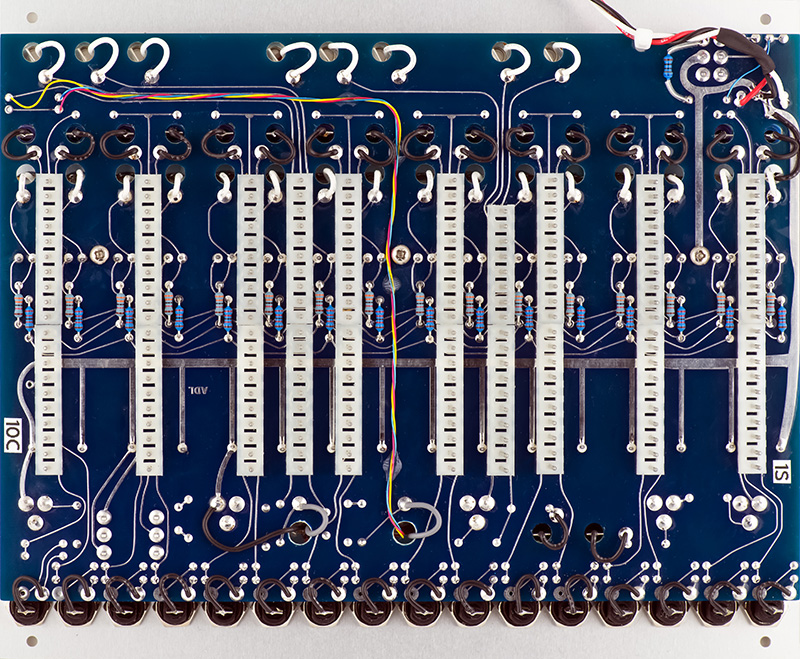
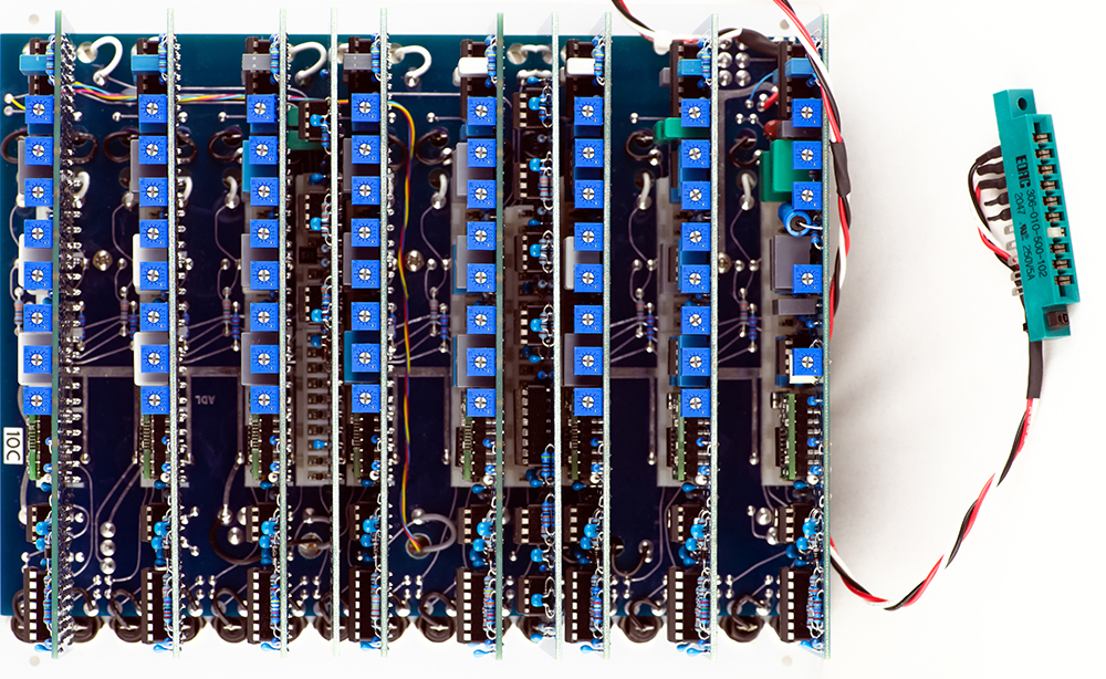
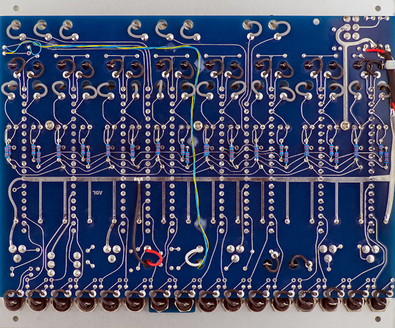
Here is the finished motherboard. The 1S and 10C labels are to remind me which way the cards install. The mods in the upper right corner were for the initial design.
The SSM2020 VCA is nearly unobtainable so I used a 2164 Quad VCA daughter card. The circuitry works out nicely where only component changes and omissions are needed on the filter cards.
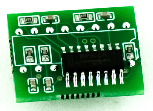
I use pins pulled from a PCB wire header which nicely match machined pin sockets used for IC3.
You need to also cut the end tab which interferes with the resistor on all the filter cards as shown by the red arrow.
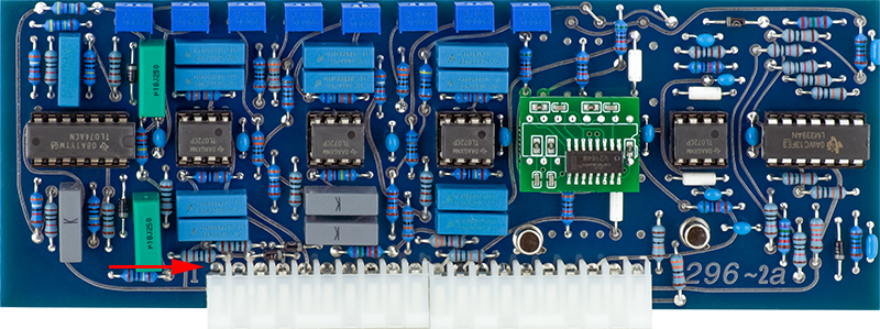
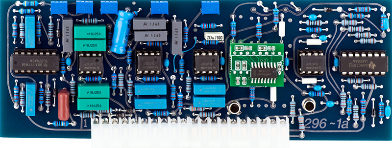
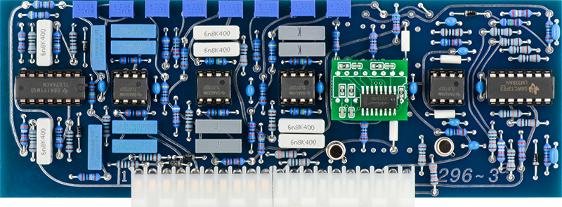
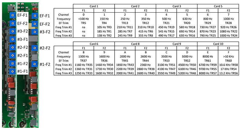
Card 1: <100 Hz lowpass and 150 Hz bandpass filters. The "white" resistors are 0R jumpers. The metal can JFET near the center of the PCB has the leads bent to mount further away from the Molex connector since the motherboard pins pass through and can short to the can.
IC5, the TL074, is used in a very high impedance circuit on all the filter cards. Very slight amounts of flux around this part can add significant offset voltage to the envelope follower outputs. Small amounts of flux can be trapped under the socket so it probably best to solder the TL074 directly in.
The resistor "buried" under the 4.7 µF capacitor is shown as a 2K2 on the schematic. It produces a gradual peak at 66 Hz with a rolloff at 100 Hz.
For comparison, the 296R does not include this resistor and its frequency scan shows a more gradual rolloff.
I chose a 1K8 which had a flatter overall response with a rolloff at 100 Hz. Note this value may work better with the tolerance of my specific capacitors.
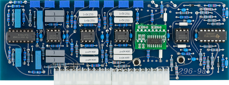
Card 2: 250 Hz and 350 Hz bandpass filters.
Card 3: 500 Hz and 630 Hz bandpass filters.
Card 4: Comb Filter and Attenuator Outputs and Program Control CV circuitry.
Card 5: 800 Hz and 1 KHz bandpass filters.

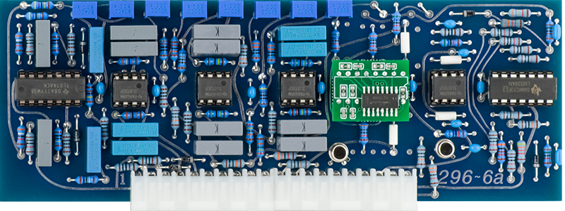
Card 6: 1.3 KHz and 1.6 KHz bandpass filters.
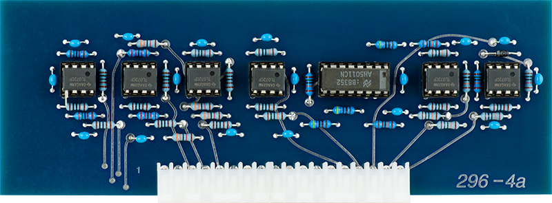
Card 7: Programmed Outputs and Envelope Follower LED circuitry.
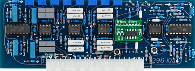
Card 8: 2 KHz and 2.6 KHz bandpass filters.
Card 9: 3.5 KHz and 5 KHz bandpass filters.
Card 10: 8 KHz bandpass and >10 KHz highpass filters.
This build is long and tedious. The filter cards take about 2.75 hours each. Cards 4 and 7 are shorter at about 1.5 hours each. The motherboard and panel takes about 3 hours and calibration takes an hour for a total of 27 hours.
296 Mouser BOM Updated
I later dyed some white switch/slider caps violet to match the banana jacks. Details are on my Modular Synths Tips page.
Low Profile Construction
A vintage 296 measures 3.19" deep on the left side top and bottom. It measures 3.23" on the right side top and 3.07" on the right side bottom. My MEMS module measures 3.125". As built per the original design, they will not fit in shallower 3" boats. My boats are from Jason Butcher and his are made deeper at 3.2" to fit modules like the 296. Here are the measurements from my module
My initial investigation into construction of the motherboard to reduce the depth is located on my 296M Programmable Spectral Processor Low Profile Investigation page. The motherboard PCB has since been revised to eliminate the interference between the rear mounted resistors and the card connectors. I have also revised and simplified my approach to installing the pins without the headers and the use of Alps 9mm potentiometers. This page is retained for reference information only.
I found that removing the plastic headers from the male pins and using 14 mm standoffs will decrease the height to fit in a 3" boat. Resistors have been moved on the motherboard to no longer interfere with the female connectors. This is how I installed the pins without headers on the motherboard. To prepare, use the round pins Mouser 538-26-20-2101 and tap the pins through flush with the header. Make a 0.115" spacer with a slot wide enough to fit around the pins. Have an extra dedicated connector to retain the pins when soldering (I chose a spare connector since it is used repeatedly for soldering).
![]()
Place the spacer around the header and insert the pins from the PCB front.
![]()
Hold the PCB flat to a surface and it will align the pins vertically.
Solder the pins on the PCB rear and use very little solder, just enough to hold the pins in place.

Remove the spacer and pry off the header.

Cut the pins flush with the PCB front.

Mount the connector on the pins to hold them in place.

Solder the pins on the PCB front.

Remove the connector. The PCB is now ready to wash (you did use organic water-wash solder, didn't you?)

The motherboard pins are now complete!

I used a 14mm Mouser 761-M1261-3005-S-12 spacer which is small enough in diameter to not interfere with any PCB traces.
I used Alps 9mm 25K potentiometers with a MEMS adapter for all the controls. This also eliminates the need for the shaft adapters for the knobs.

Without the headers the female connectors on the cards slightly interfere with many of the 33K resistors which are close to the rear of the cards. You need to trim off the two plastic tabs between pins 10 and 11 on all cards.
Unrelated to the lower profile, you need to also cut the end tab which interferes with the resistor on all the filter cards as shown by the red arrow.
This is the panel all wired and ready for assembly with the motherboard.
Here is the completed low profile motherboard which will fit in a 3" deep boat.
I chose to not try and find a new old stock AM97C11 or one of the equivalent ICs for IC10. Don used this simply as four p-channel JFETs so I used four discrete J176 JFETs (Mouser 512-J176D74Z). They worked very well for the program control and it is dead quiet when sweeping the bandwidth and frequency controls.

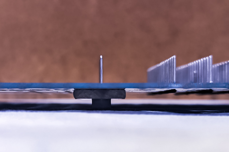
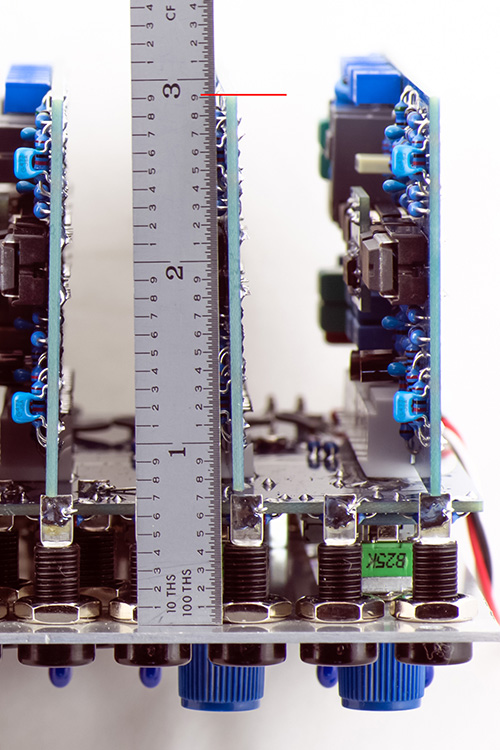
This side view shows the minimal clearance between the Alps 9mm PCB adapters and the motherboard. I trimmed all the leads flush with the rear.
![]()
It's a bit hard to see the clearance so this close-up is more clear. I also used internal tooth washers on the potentiometers which made it more difficult to assemble. Omitting those would increase the clearance a bit.
![]()
The depth of the module is 2.92" so will fit in a 3" boat. Make sure there are no screw heads beneath it.
Here is the low-profile 296 rear. I wire tied the power cable to a banana jack hole for strain relief.

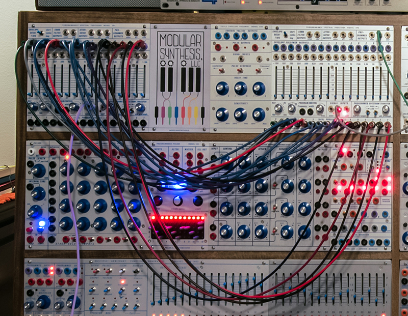
Here is the low-profile 296 on the left as part of a full vocorder patch.
Calibration
Calibration is straightforward. Use a DMM on the individual channel output and adjust each to <2mV with no signal inputs. If you can't get them to this level then sometimes excess flux on the PCB can be the cause. Do all 16 channels first.
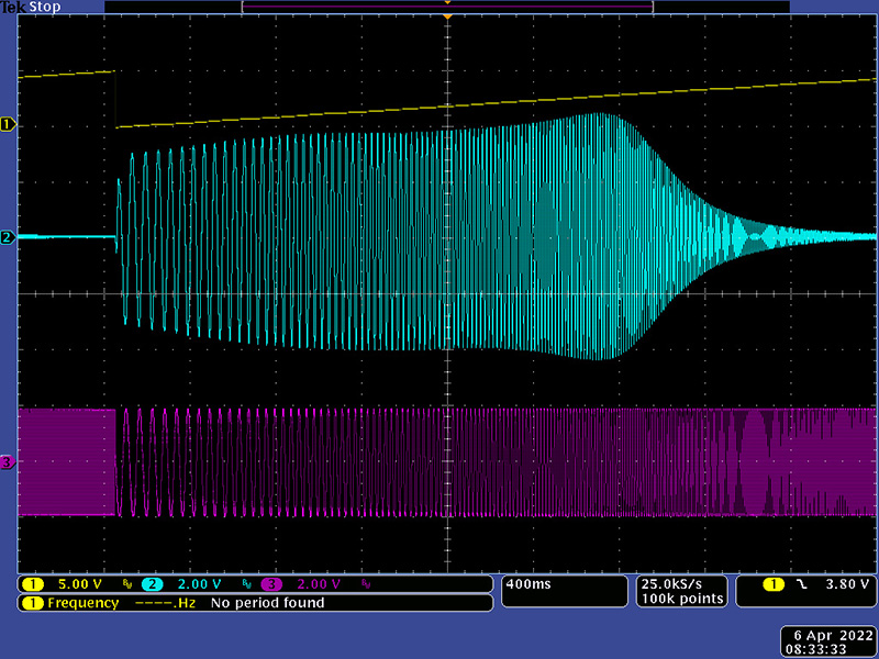
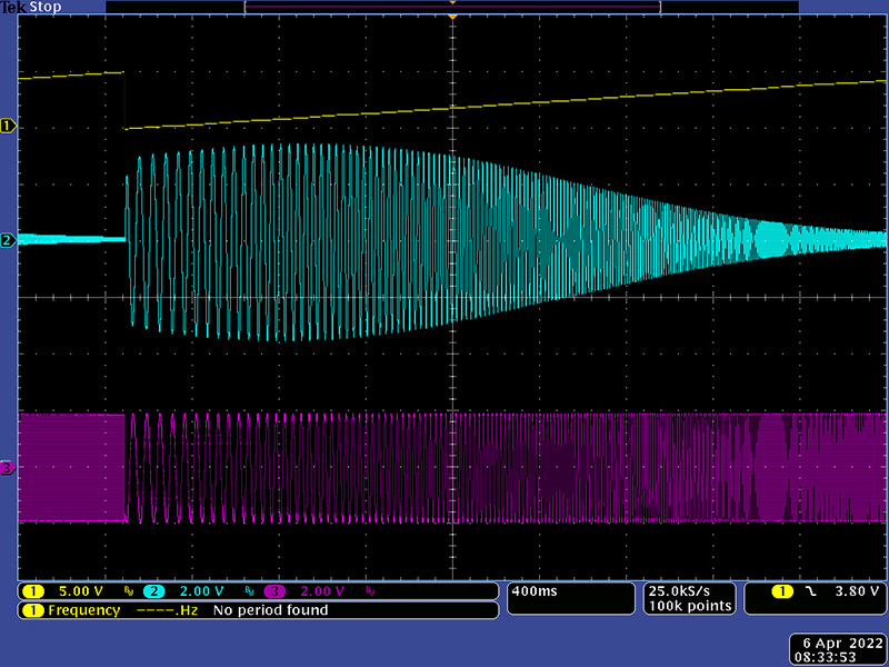
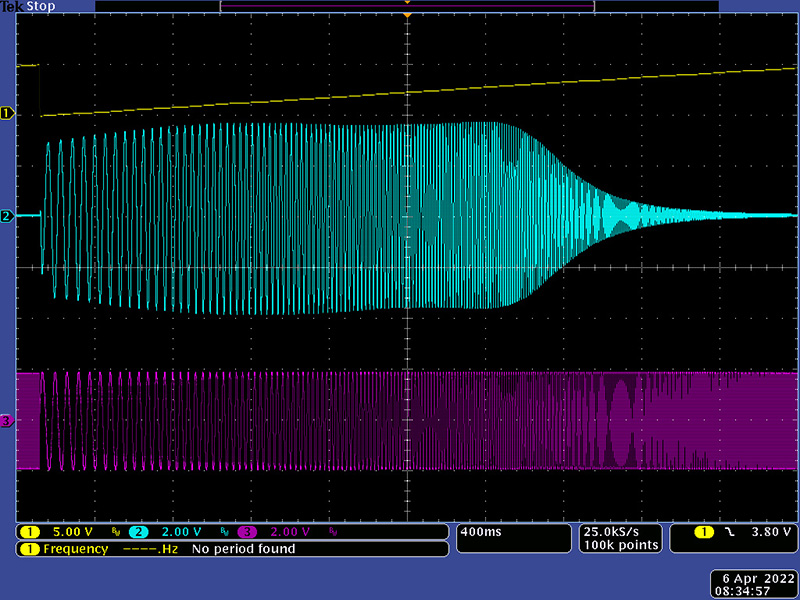
The filter topology is designed around three cascaded single op-amp multiple feedback bandpass filters in a stagger tuned configuration. Each of the filters is a small frequency offset from the next to get a wide and flat passband with steep slopes. You adjust each of the three filters for maximum output at their specific frequency.
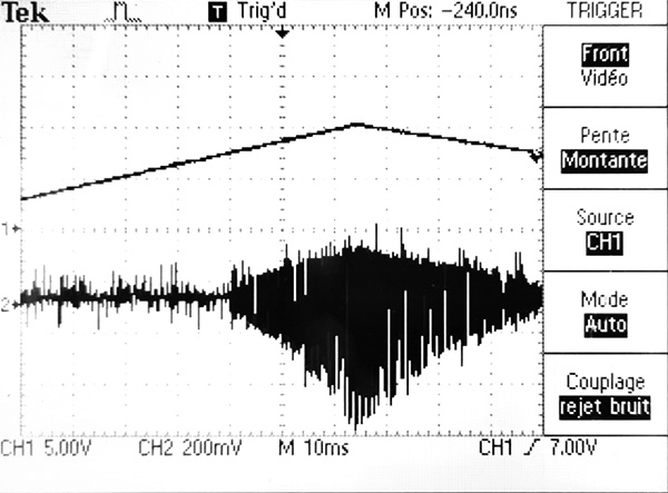
There are three trimmers per channel except for the <100 Hz channel. To adjust the frequency trimmers, monitor the individual filter output with an oscilloscope and apply the correct frequency input. Keep the pre-emphasis knobs at minimum (full
CCW). Adjust the trimmer for maximum amplitude. The amplitudes will be different since the other trimmers for that channel may not yet be set. Also, there is some variation in overall amplitude between channels. (Note - if you have a two channel oscilloscope then monitor the output of your signal generator and trigger on channel 1 and monitor the individual filter output on channel 2. This will make the display a bit more stable).
There is a regular pattern to follow for calibration. Set the input frequency to what is shown for Trim #1 and adjust, then set the frequency for Trim #2 and adjust, and then set the frequency for Trim #3 and adjust. Then repeat for the second channel on that card. You soon learn the pattern of adjusting the lowest trimmer, then moving up two, then moving up two, then going to the next to the lowest trimmer, then moving up two, then moving up two. I kept a marker on the card I was adjusting so I didn't venture to either side which is easy to do. Calibration is pretty quick.
For those that do not have a calibrated waveform generator for the calibration, SAModular has recorded wave files that you can download to use.
Operation
This 296 calibrated quite easily. There was no noise on the Programmed Outputs and the Frequency and Bandwidth controls operated smoothly. I've seen these issues on some of the clone modules and corrected them by adding more decoupling. The original design had more decoupling and wider power traces. This is a great sounding and operating module.
SSI 2164 Parts
An individual contacted me whose 296M exhibited noise on the program outputs when the Width potentiometer is full CW. The noise was oscillation around 700 KHz and was more noticeable with SSI than Alpha 2164s. It might have been impacted by the switching power supply. It turns out the control TL072 op-amps were oscillating. He stated increasing C8 and C17 from 100 pF to 220 pF corrected the issue.
I used SSI 2164 parts in my Low Profile built above. I found considerably worse results. I verified card 1 as soon as complete, so the module consisted of cards 1, 4, and 7. I had significant 'chopping' on the programmed output when using either the Program controls or an external CV. Increasing these capacitors did not correct this issue.
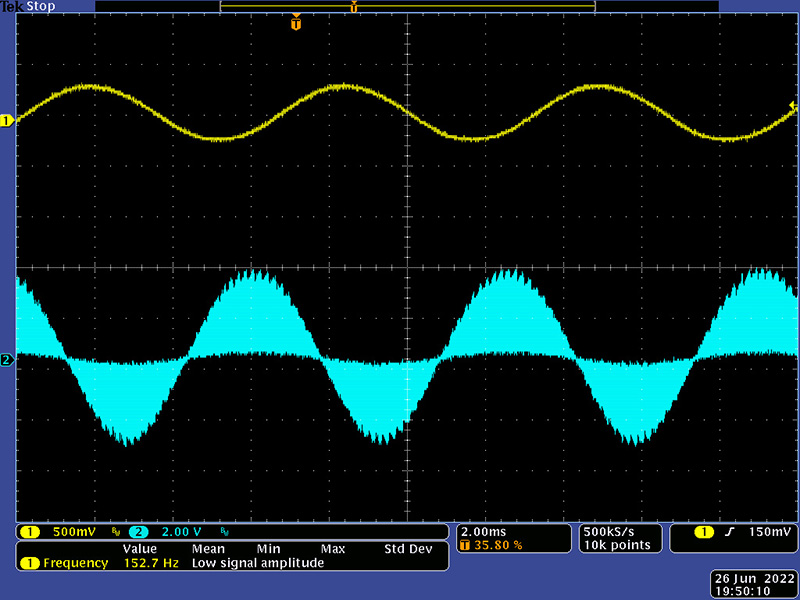
This chopping is full amplitude and occurs at about 45 KHz, so a considerably different frequency than he noted.
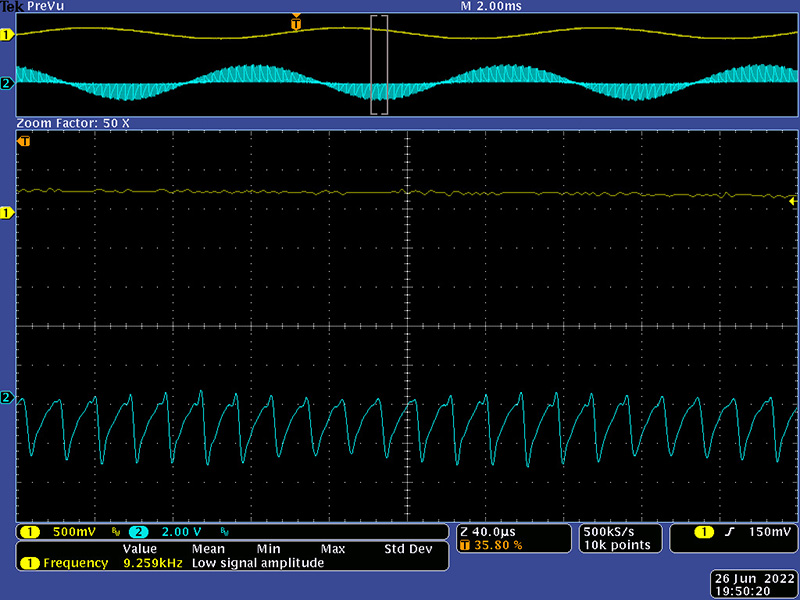
I modified the adapter card to the standard 220R and 1200 pF compensation network. This eliminated the chopping but now there is a negative DC shift in the programmed output at CCW setting of either Frequency or Bandwidth control. I verified this offset does not occur with the Coolaudio 2164 parts.
I then calculated the compensation network for the input impedance per the SSI datasheet. The audio channel requires 750R and 330 pF and the reference channel requires 180 pF and 1K4. Using these values with verification on a single card seemed to function correctly.
I changed all 64 0603 parts and I have no oscillations when just using the program controls. I do, however, still have significant (e.g. several volts) of DC level shift as I rotate the Bandwidth control. I tried to isolate the channel by turning on each VCA individually. In many of the channels, they break into oscillation at the maximum CV level and many have some amount of DC level shift. This is just becoming too much work to address when the Coolaudio parts work just fine. I recommend to NOT USE the SSI2164 parts based on this experience.
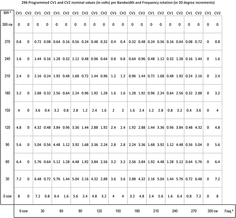
The Programmed CVs always seemed a bit mysterious to me so I mapped them out better. These are calculated values for edge pins 16 (CV1) and 17 (CV2) but come pretty close to what mine read (although I didn't do a comprehensive check). The nominal range is 0 to 8V and I suspect the voltages depend what IC was used for the AMC911 on card 4.