|
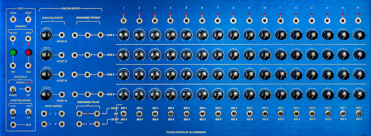
Milton Sequencer Module |
|
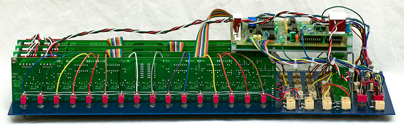
A customer sent me a populated set of Milton boards to build into a sequencer. It came out very nice. I configured this module for a 10V CV output range on +/-15V operation. The power consumption is 120 mA of +15V and 90 mA of -15V (all LEDs lit).
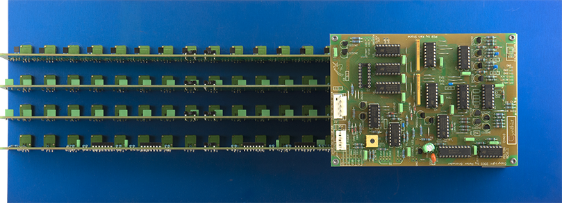
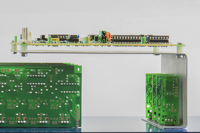
My first task was to determine how to mount the engine PCB. I drilled the potentiometer holes and installed the bank and offset boards.
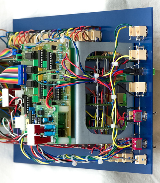
I decided to make a bracket that would mount behind the offset potentiometers and tie into the bank board mounting holes. The engine board mounts on the back and the depth is 4.5"
This bottom view shows how the bracket fits. I still need to make short brackets to attach to the bank board mounting holes and cut the side of the bracket for access to the offset boards.
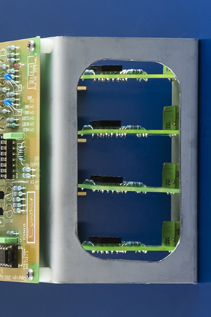
I used a chassis punch to cut the four corners and used a Dremel cutoff wheel to cut the center out. This cutout provides good access to the offset boards.
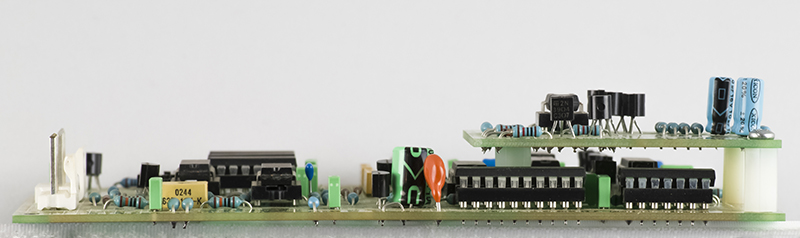
I drilled the engine board to mount the ACB board securely with standoffs.
The extra two holes line up perfectly with ground planes so I used nylon hardware.
The ACB board sits nicely on top of the engine board.
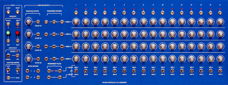
This is the assembled panel and the NKK HB series illuminated momentary push buttons for Run and Halt are very nice.
I mounted the stage LEDs to a bus bar that I epoxied to the top of several jacks. I added a socket for R23 so the stage LEDs could easily be adjusted for brightness.
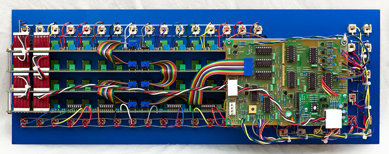
The LED common bus bar is visible in this photo. You can also see color coded wires to each stage jack.
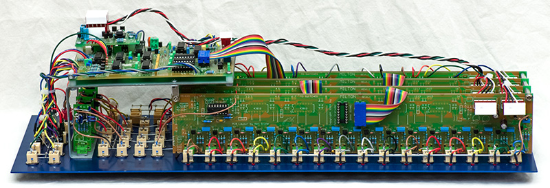
There are a lot of wires coming from the engine board that make assembly a bit challenging.
You can see the offset boards through the bracket cutout. I bused power and grounds with insulated wire as there was no provision for daisy chaining power. I later rotated the MTA connectors on the ACB board and used a feed-thru MTA housing since the connectors are so close together.
Modifications
I added a mixer after the attenuverter on the offset board so it can be used to offset the Bank outputs. I used 0.1% resistors since these are control voltages. The extra of jacks to the right of the Offset In jacks are the mixer inputs which are normalled to the Bank outputs.
I modified the Disable circuit so it requires an active high signal to disable the programmed pulses. I added the unused inverter U5 pins 10 and 11 before the input to U9 pin 8. This required cutting runs from U9 pin 8 and wiring them around and also cutting the run to U5 pin 11. Since it is a wired 'OR' active high signal the manual switch can be used to enable and the jack can override to disable programmed pulses.
I added a LED to indicate Hold. I used a 2K series resistor from the collector of the 2N2222 to the cathode of the LED and connected the anode to +V.
I changed the resistors for a 10.1V output for the Bank CV. I used the following resistor values (left to right): 665K, 93K75 (100K||1M5), 102K, R1=100R, R2=0R. The CD4050 buffers have to source 1.2mA for the bank controls and have nearly a 1V drop from Vcc.
I changed the resistors for a 10V output for the Programmable Pulses. I used the following resistor values (left to right): 6K65, 10K, 10K, R3=R5=100R, R4=R6=0R.
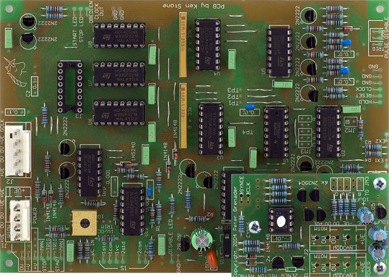
The output of U5 pin 9 is pin 8, not pin 10 on the engine schematic but the PCB is correct. Pins 12 and 13 of U12 are swapped on the schematics and rev 1.1 PCB.
I added the 10K pulldown resistor on the emitter of the 2N2222 transistor in the obedient clock output. This is mentioned in the testing notes.
I changed the 1K8 resistor on the comparator to a 2K trimmer to be able to trim in the threshold. It needs to change to 1K4 for a 0.20V threshold for 15V operation.
I changed the V/O trimmer from 10K to 50K. I could tune the Kybd input to track a keyboard only at the far extreme of the range. The gain was 1.9 to 2.1X and I changed it to 1.67 to 2.5X.
I changed various resistor values to even the luminance of the various LEDs. The resistors ranged in value from 1K to 20K for the high efficiency blue LEDs. Most were 2K.
U2 pins 3 and 5 connect to the virtual ground node on U1 pin 9 and U2 pin 2 on the Bank board. The Programmable Pulse LEDs will NOT operate since this point is always at 0V. I cut these runs and wired U2 pin 3 through a diode to G1 and U2 pin 5 through a diode to G2. I added a 100K resistor and 0.1 µF capacitor from U2 pins 3 and 5 to ground to stretch the pulse for the LEDs. It makes the blinking LEDs a brighter and blinking is visible up to a 25 Hz Clock.
Operation
There are quite a few different modes for the Milton. In Std mode the Clock will advance the sequencer while the VC input is below 0.2V. When the VC input is above 0.2V the Clock is inhibited from advancing the sequencer and the VC selects the stage. The Clock still generates Programmed Pulses and in Sync mode the Obedient Clock follows the Clock input. If set to Async the Obedient Clock follows the stage selected by the VC input.
In Kybd mode the Clock is inhibited from advancing the sequencer and the VC input selects the stage. The VC gain is increased and adjusted with the trimmer. The Programmed Pulses and Obedient clock act the same as in Std mode.
The stage gate outputs and the Obedient Clock output in Sync mode are ~15V levels. The Obedient Clock output in Async mode is 10V if the zener is installed.
Bank and Offsets
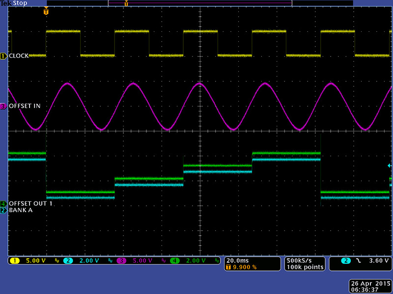
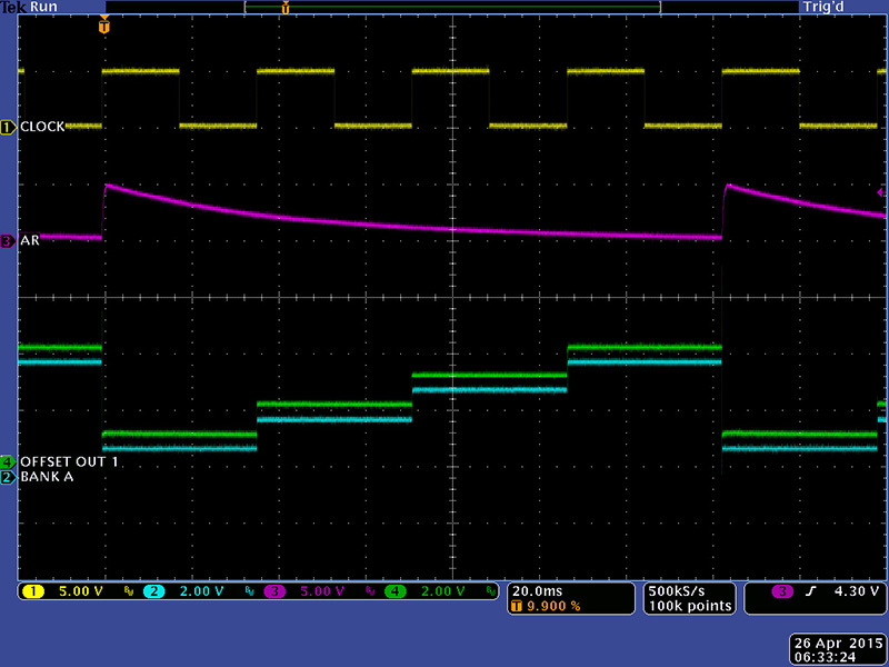
This image shows a simple 4 stage sequence created by patching stage gate 5
into reset. Bank A is set to 1V steps. A sine wave is patched to the
Offset In but the Offset attenuator is set to midpoint so there is no offset
added. I've slightly offset the Bank A and Offset Output 1 traces so you
can easily see they are the same.
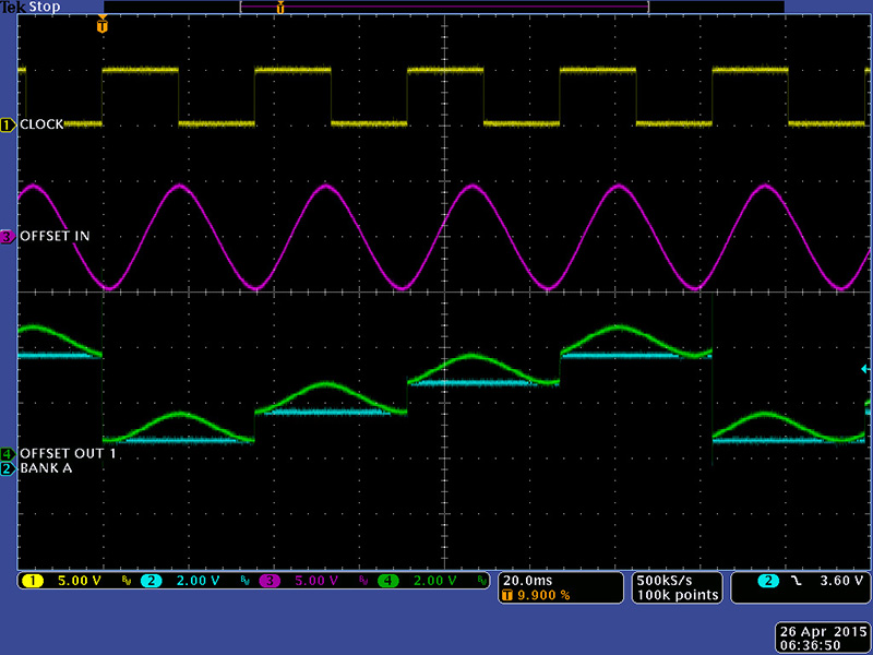
In this image I have added a slight positive offset and you can see how Offset Out 1 is the sum of Bank A and the Offset In.
I have programmed Bank B to output a 5V pulse at stage 1 to drive an AR that is now patched into Offset In which is set to midpoint so there is no offset added. Again you can see Bank A and Offset Out 1 are identical.
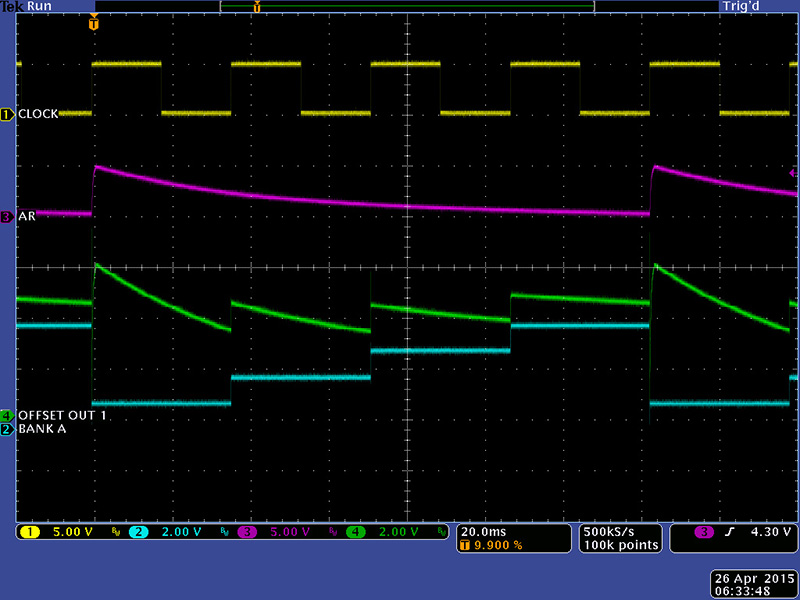
This image shows the addition of the AR offset to Bank A at full positive rotation.
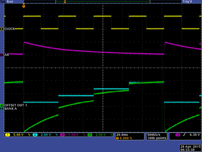
This image shows the addition of the AR offset to Bank A at full negative rotation.
Obedient Clock and Programmable
Pulses
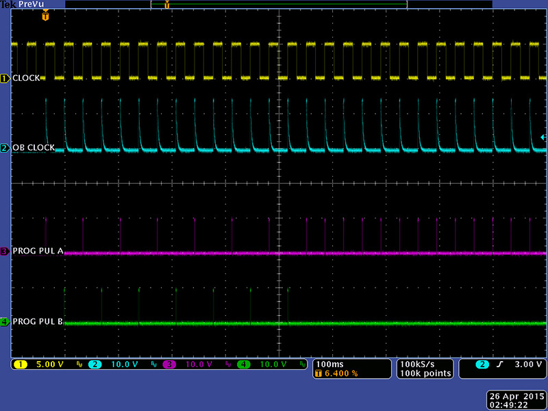
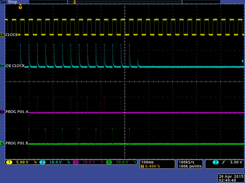
This image shows clock operation with
no VC and stage 16 patched back to hold. The Obedient Clock is set to Sync
and is output on every clock edge. The Programmable Pulse switches are set
on alternate buses for each stage. Since it holds on stage 16 and that
Programmable Pulse is set to Bus A that pulse occurs on every clock after it
holds.
This image shows stage 16 patched back to Halt. Since the sequencer stops the Obedient Clock outputs also stop. Note the truncated Obedient Clock at the end of the cycle. This is typical of asynchronous designs and is due to clock that halts the sequence is the same clock that gates the Obedient Clock.
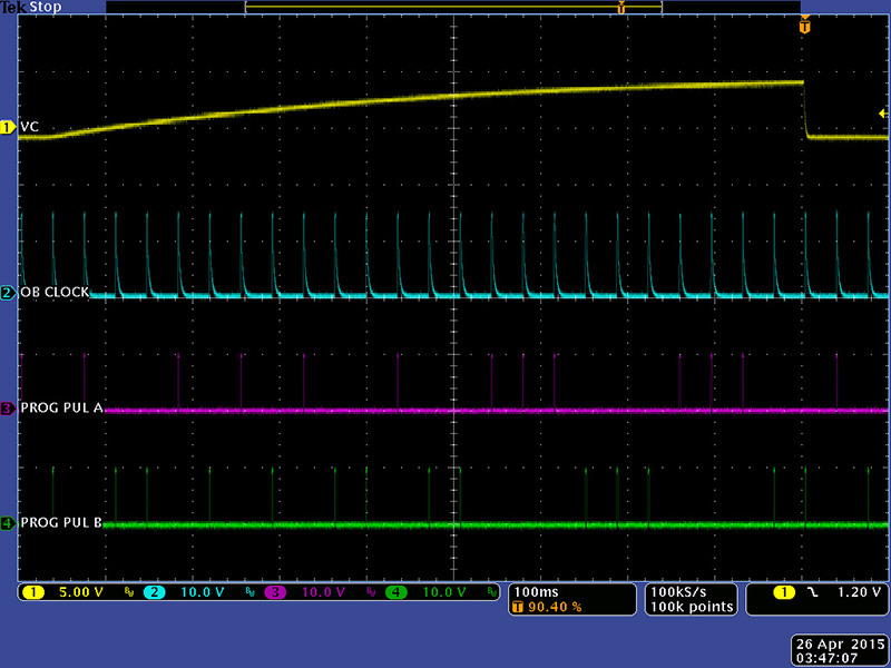
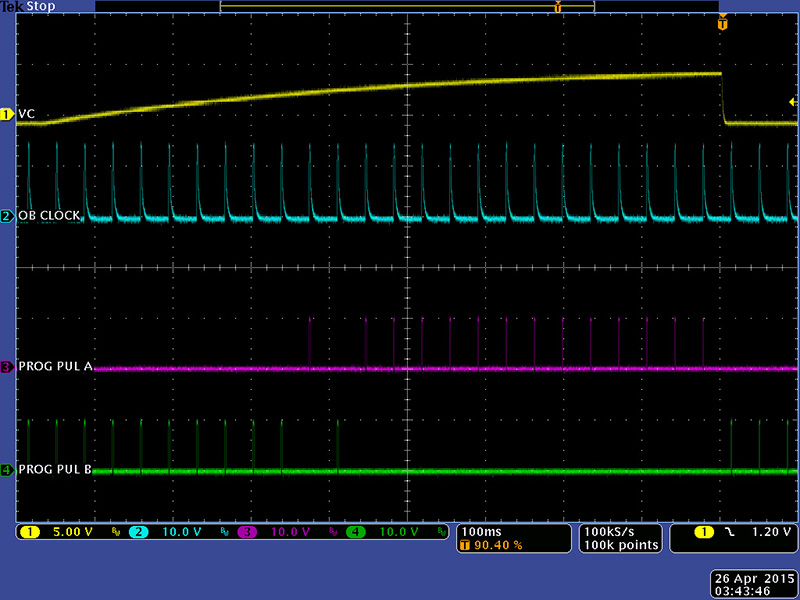
This image shows the VC operation driven by an AR with no clock input in Std and Async mode. Since there is no Clock there are no Programmable Pulse outputs.
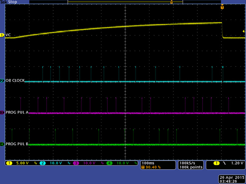
Switching to Kybd mode increases the VC amplitude internally so the Obedient Clock outputs occur earlier in the AR cycle.
Zooming in on an Obedient Clock shows the 2 mS width although in the two previous images the Obedient Clock at the falling edge of the VC was wider. I believe this is due to the software algorithm filtering ABCD glitches as the DAC transitions from stage 16 (ABCD=1111) to stage 1 (ABCD=0000).
.jpg)
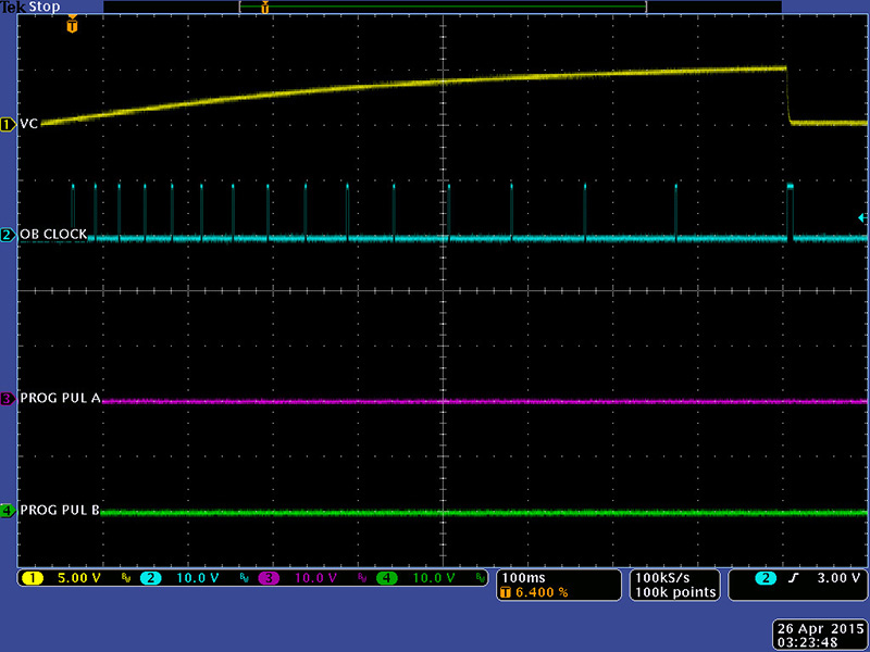
This image shows the Obedient Clock tracking through all 16 stages with a 64mS ramp VC. Again note the wider clock width at the first stage. All 16 stages are sequenced within about 54 mS and the Obedient Clock output is valid at that rate.
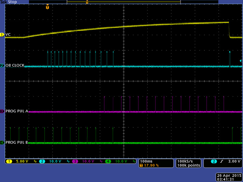
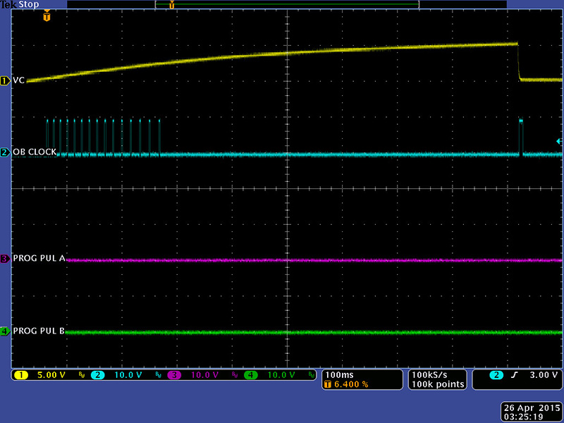
I have increased the ramp frequency so all 16 stages are sequenced in about 46 mS and one Obedient Clock has dropped out so the upper limit for tracking a VC through 16 stages appears to be ~54 mS. I do not know if this is due to the filtering that may be going on in the software or the speed of the PIC processor. I did design a quick design of an AVR plug in processor that could track ABCD changes very quickly with a much shorter Obedient Clock output. With it the transition from stage 16 (ABCD=1111) to stage 1 (ABCD=0000) did generate a number of false Obedient Clocks so I am pretty sure the PIC has some type of filtering algorithm.
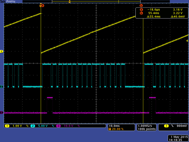
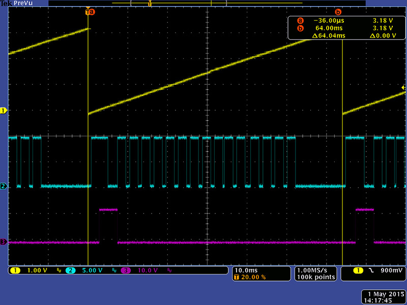
Things get more complicated when you combine VC mode with a clock. This image shows an AR input that is slightly shifted negative. In Std mode the VC threshold is 0.2V and the Obedient Clock follows the Clock input. The Programmable Pulses no longer alternate symmetrically because they occur when the VC input has selected a stage and is in that stage when a Clock occurs. Since the VC input is not time correlated to the Clock the sequencer is advancing stages independent of the clock.
The Obedient Clock follows the stage when set to Async mode. You can see where there are multiple clocks between Obedient Clocks as the Programmable Pulses will have multiple outputs correlating to the multiple clocks occurring at that stage.
Switching back to Sync and selecting Kybd mode now has the Obedient Clock following the Clock and the Programmable Pulses occur on each clock depending on what stage has been selected by the VC.
Finally, the last mode is Kybd and Async where the Obedient Clock follows the stages. Again, the Programmable Pulses occur based on the selected stage and the clock.