 |
Oberheim SEM |
|
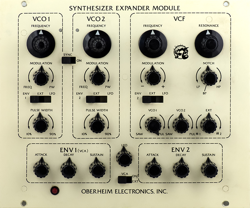
The Oberheim SEM was a synthesizer expansion module designed to be an accessory to connect to a sequencer or another system. This particular SEM came in for repairs and the date codes on the ICs are 1976. It had a number of problems that required repairs to the power supply and VCOs but otherwise is in quite good condition.
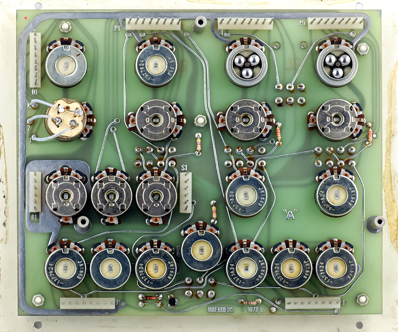
The fine tune control is implemented with a ball bearing reduction drive that is built into the potentiometers.
All of the external connections are made by 3 pin Molex connectors. At the bottom are a number of jumpers for configuring the envelope generator options.
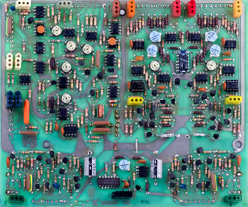
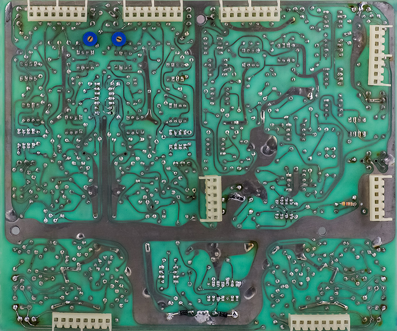
Here are the locations of the various SEM trimmers, jumpers, and connectors.
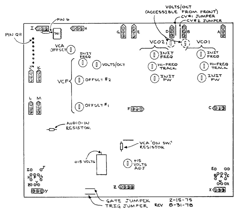
Oberheim SEM trimmers & jumpers PDF file
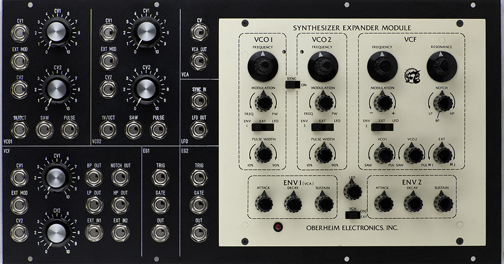
My customer wanted this SEM made into a Dotcom panel. There is an 8MU panel design is on Muffwiggler topic Rack Mount Tom Oberheim SEM ? but I chose to design my own panel using MOTM style fonts and tic marks. I added one more CV input to each VCO which requires adding a resistor and wire to the SEM. I also normalled the VCA CV input which requires lifting R179 and wiring it to the front panel jack. The Envelope Generator jacks are normalled to operate as they do on the SEM with Trig normalled to Gate, and EG2 normalled to EG1. VCO1 1V/Oct is also normalled to VCO2 and the VCF CV2 inputs. Note the SEM is powered by +/-18.5 volts so it either needs a special power supply or conversion. See below for details.
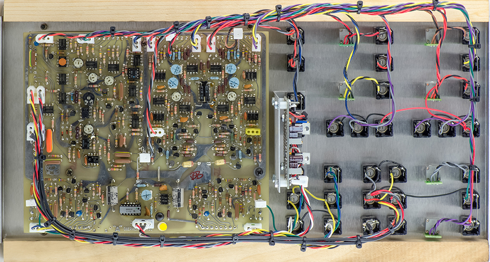
This took over 4 hours to wire. There are 31 jacks and 6 potentiometers. I used shielded cable for the VCF external inputs and twisted pairs for all of the other wiring. I soldered three pin headers to the ground run with the middle pin lifted to connect to the three additional resistors. You can see the two MTA connectors, two on the upper right edge and the third just below center. These are for the additional CV input and the normalization for the VCA CV. The board across the bottom is a stiffener while I worked on the panel as the SEM is pretty heavy. This image was taken before I added the CV normal wiring and changed the EG normal wiring (see EG below).
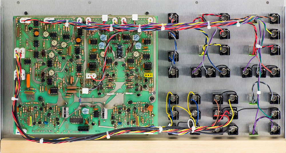
There are two sets of two jumpers that have to be removed. The top set connect the two sets of CVs between VCO1 and VCO2. The bottom set connects the two EGs together. On each lower corner are the EG jumpers which are set for Trigger and Gate. Only these jumpers should be installed: X-C, W-A, B-E, Z-H, Y-F, and G-J.

Envelope Generator
While most of the functions are straightforward, the Envelope Generator is a bit different. The SEM EG is jumpered to operate gate only which internally generates a trigger as can be seen in this scope image. The internal trigger is a 15V trigger while I am driving the gate with a 5V signal.
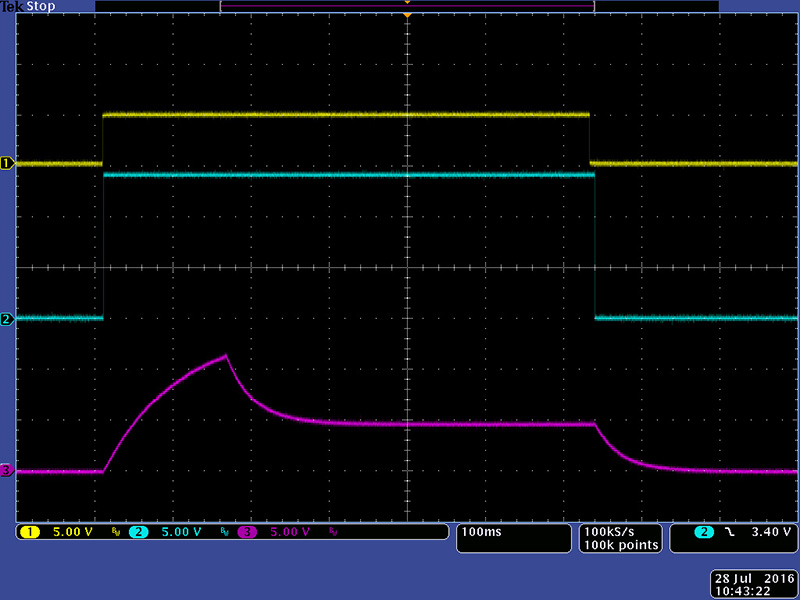
The two transistor buffer provides about 1.1 mS of delay between gate and trigger.
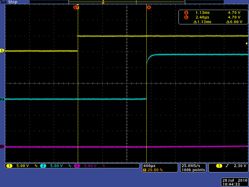
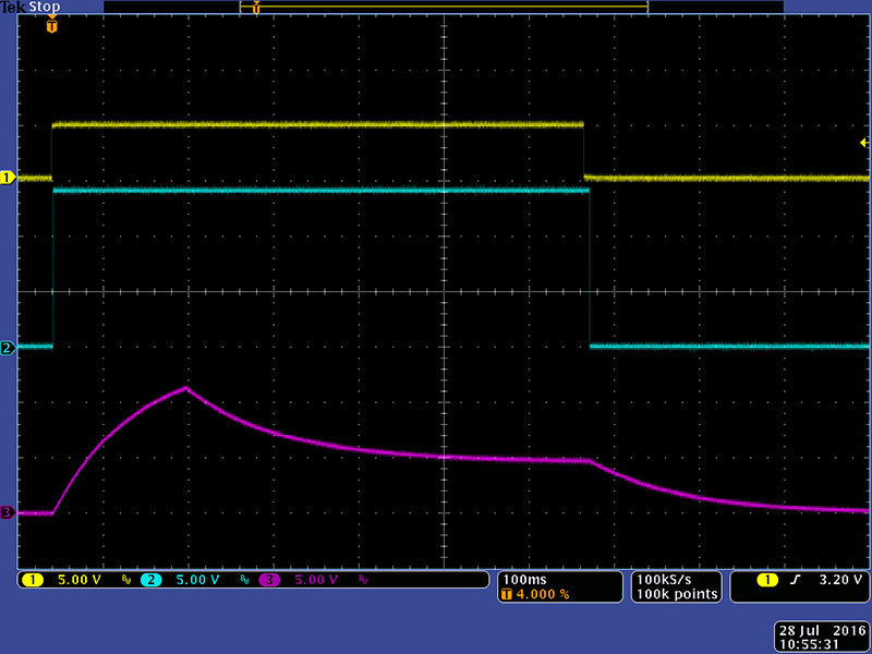
Without this delay, the envelope generator does not operate properly. I am driving the SEM gate and trigger from my modified ARP 3604-P keyboard which has 10V outputs but synchronized gate and trigger. In this scope image you can see that the attack only goes to the sustain level. Trigger is what "kicks" the output up to maximum so it can decay to the sustain level and must be delayed from gate approximately 1 mS for the envelope generator to function properly.
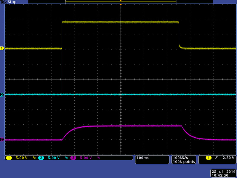
This scope image shows the trigger delayed through my DJB-008 Dual Trigger Delay module of which the minimum trigger delay is 50 mS. You can see the output start to attack up to the sustain level and then the trigger "kicks" it up to the maximum level.

This scope image shows the retrigger capability of the SEM EG.
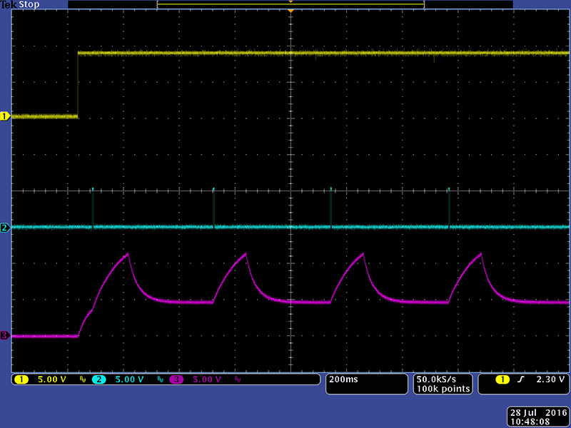
While this is an ADSR EG, there are only three controls. Decay affects both the Decay and Release timing. This scope image shows the Decay set to zero.
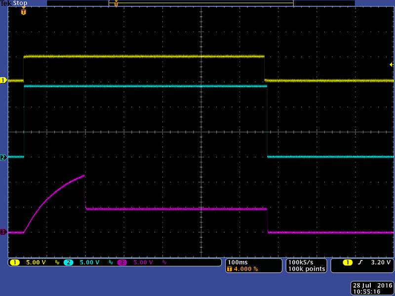
This scope image shows the decay set to non-zero.
Power Supply
The SEM requires regulated +/-18.5V. It is re-regulated on the PCB to +/-15V for most of the logic but the VCO cores use +18.5V. I can only surmise that this was done to provide another degree of isolation between the VCO core and other switching signals like the Envelope Generator and the LFO. The VCO cores could probably be converted to +15V but then one would have to investigate any resulting issues. The +/-15 volt regulators would also have to be bypassed requiring modifications to the PCB.
Option 1: Use the SEM Power Supply
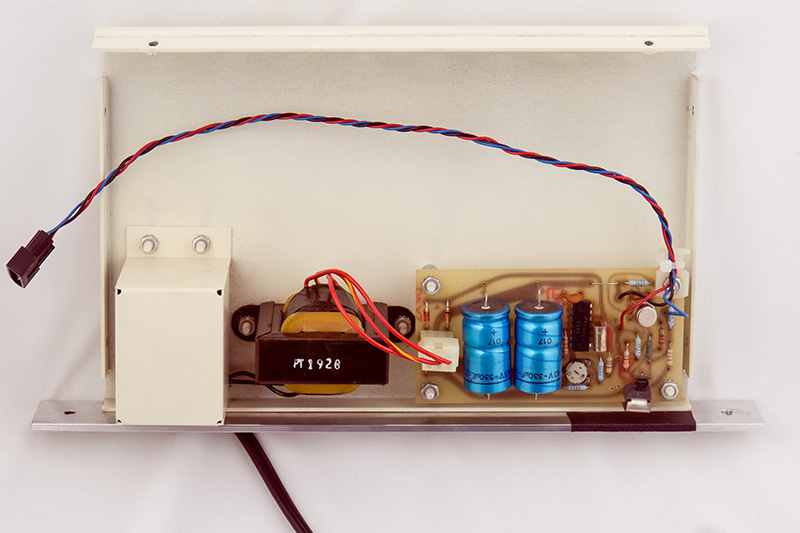
The power supply is mounted on the rear panel of the cabinet. This can be easily removed with four screws and used as a power supply for the SEM. The advantage is it is simple but the disadvantage is the extra AC power cord and switch. I removed the 3.5mm jacks and wires, a 4K7 resistor on the power supply for normaling the VCA, added a strain relief for the DC power cable, and made a bracket for the bottom to mount the power supply panel. The tabs on both TO-220 power transistors had been bent over so I added tape on the bracket for increased insulation.
Option 2: Use a +5V Supply
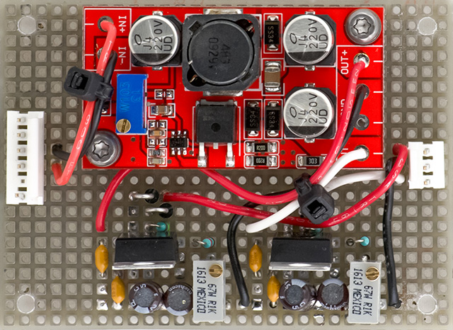
This DROK DC Boost Converter is available for a very reasonable price. However, these type of converters have a lot of noise so I added a LM317/LM337 linear regulator after it. I set the DROK to +/-21 volts and adjust the LM317/LM337 to +/-18.5 volts. I chose to build the linear regulator PCB but one can find many PCBs or kits on Amazon or eBay for a dual supply built with these regulators. You just need to leave out the bridge rectifier and filter capacitors and possibly change some resistors to be able to adjust to 18.5V.
Without the EGs or VCA operating, the current draw was 70 mA of +18.5V and 45 mA of -18.5V. Assuming 6 mA consumption for each linear regulator and 85% efficiency for the DROK, this requires 640 mA of +5V.
The output of my DROK was a bit asymetrical so when I adjusted the negative supply to -21V the positive supply was a bit higher at +21.6V. Total consumption measured 650 mA at +5V, close to my calculations.
This power supply board is setup to use the +5V from a Dotcom system. For testing purposes I simply used a 1A USB supply which worked quite well.
This scope image shows the noise from the output of the switcher (cyan) and the significant reduction in noise on the +18.5V output (yellow).
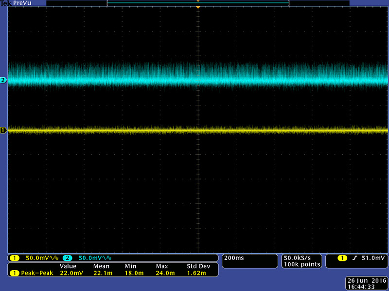
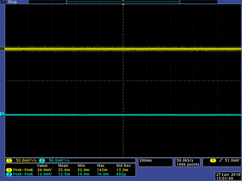
This scope image shows the noise on the +18.5V output (yellow) and the slightly lower noise floor on the -18.5V output (cyan).
This image shows the rear panel wiring with the power supply mounted in the center. On this panel you can see the CV normal wiring and the two additional MTA jacks at the bottom sides for the EG normal wiring.
I helped Tim Hill with a similar project by sending him several high resolution photos of the module and wiring. He sent me back this image with all of the reference information for the connectors, controls, and jacks added. A link to a high resolution image PDF is below.
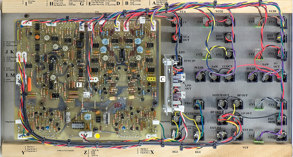
High resolution rear reference information
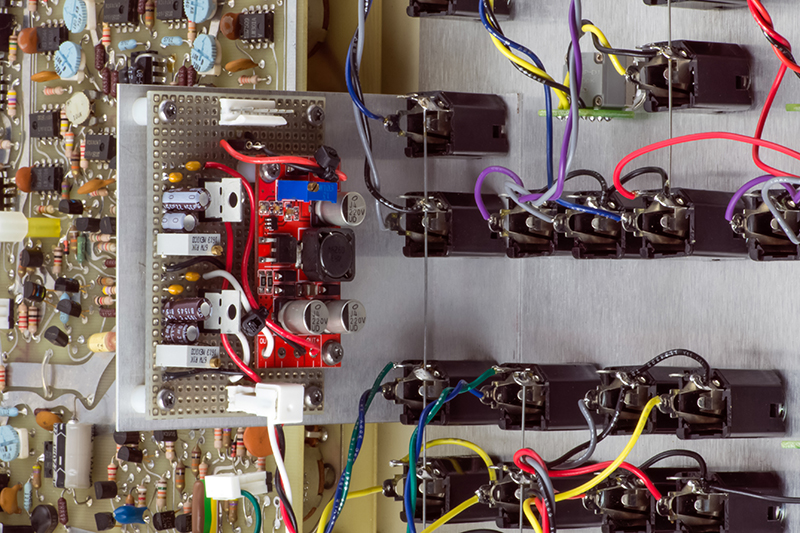
This image is a close-up of the power supply. The socket just below the Dotcom connector is for a fuse (with a wire link in this image).
Here is a photo of the SEM installed in the customer's synth.
