I don't own a Papareil Synth Labs Quantix-8
CV quantizer / wavetable oscillator module but have repaired them. There is some discussion
of the Quantix-8 on the Electro-Music
and Muff's Modules
forums. This is a
very interesting module with multiple modes of operation. The inclusion of
PC software for editing and creating the waveforms makes this a very useful
module.
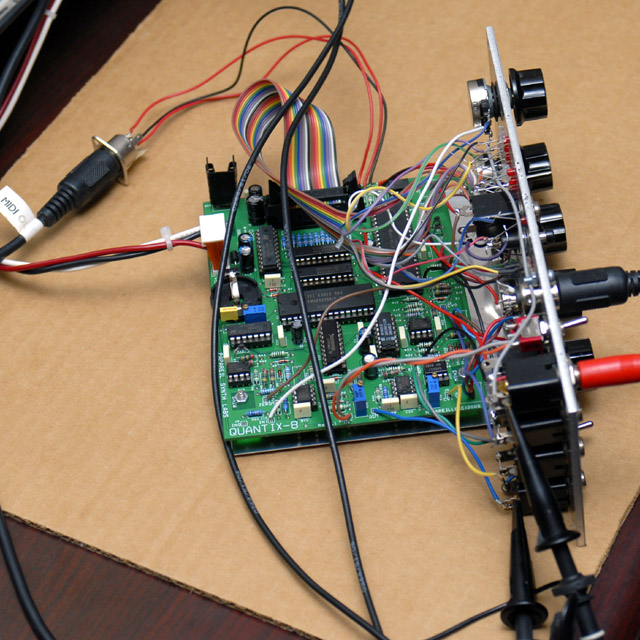
Quantix-8
This particular module had garbled output which I traced to erratic
operation of the LTC1099 ADC. This ADC generates the lower 8 address bits
for the waveform memory from the input ramp waveform. In this image you
can see the ramp input waveform (magenta) and the processed ramp input to the
ADC (yellow). The bias control is adjusted correctly to produce a zero
output at the beginning of the ramp waveform. The DB0 output (green)
should toggle uniformly throughout the entire waveform to correctly address the
LSB of the sample memory. The other seven output showed similar erratic behavior.
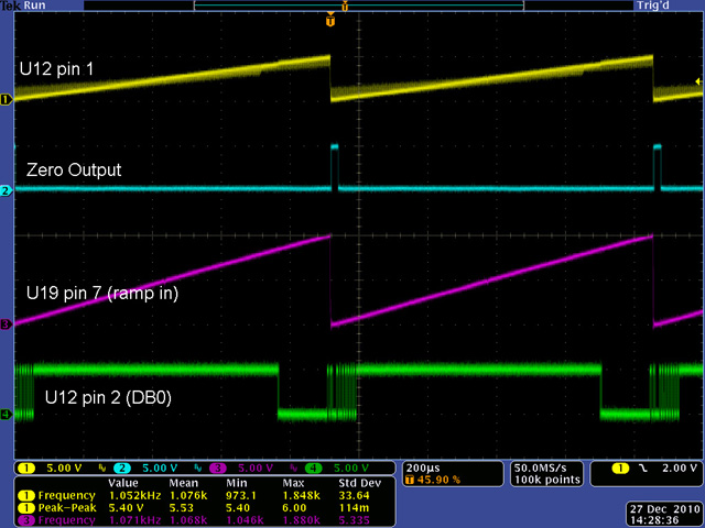
I traced the output problem to the clock frequency which was up
over 600 KHz . The conversion time of the
LTC1099 ADC is specified at 2.5 µS and lowering the
clock frequency to 400 KHz established reliable operation. Proper adjustment of the
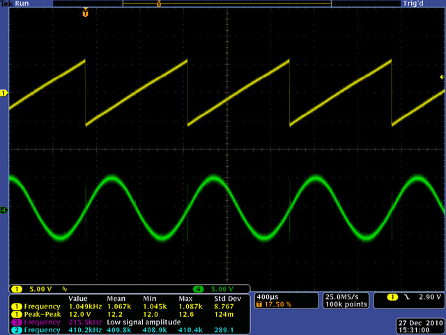
input attenuation and bias controls are necessary to produce a uniformly continuous
waveform as can be seen in this image of a sine wave output.
Quantix-8 Tips &
Modifications
-
The
LTC1099 ADC has a specified conversion time of 2.5 µS which is 400
KHz. I replaced C6 with a 4n7 capacitor and adjusted the 4093
oscillator frequency to 400 KHz to for proper operation of the input
ramp ADC.
-
The
Gate I/O jack should be wired to J4 which connects to pin 24 of
U15 (this is in error in V1.1A documentation but correct in V1.1B
documentation). I added
over/under voltage protection for the PIC with a 1K resistor in
series to the jack and a diode to ground and a diode to +5 volts on pin 4
of U15. The PIC spec is +/- 0.3 volts so you might want to use
schottky diodes for a low voltage drop.
-
The
Zero Out jack should be wired to J3 which connects to pin 4 of U15
(this is in error in V1.1A documentation but correct in V1.1B
documentation). Although
this is an output, I also added the same over/under voltage protection for the
PIC with a 1K resistor in series to the jack and a diode to ground and
diode to +5 volts on pin 24 of U15. Again, you might want to use
schottky diodes for a low voltage drop.
-
The Zero Detect LED
is wired with the anode connected to +5
volts and the cathode connected to J11 pin 16 (this is in error in V1.1A
documentation but correct in V1.1B documentation). You adjust the +/-5 volt
ramp input level and bias until both the Zero Detect and Overload LEDs just begin to
flicker.
-
The
values for R58 and R36 are shown
incorrectly on the V1.1A and V1.1B implantation schematic (e.g. component
values). R36 is 5K (is shown as 10K) and R58 is 10K (is
shown as 100K).
-
I
could not reliably transmit to the Quantix-8 on my Windows XP computer
and received the error message: The port is transmitting data to
the device. Wait until the data has been transmitted, and then
try again. Increasing the Sysex Send Delay to 30 resulted in
reliable communications for my computer.
|
back
