|
208 V2 Stored
Program |
|
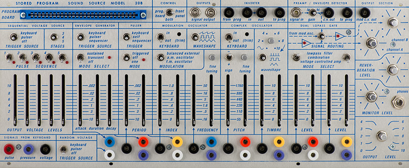
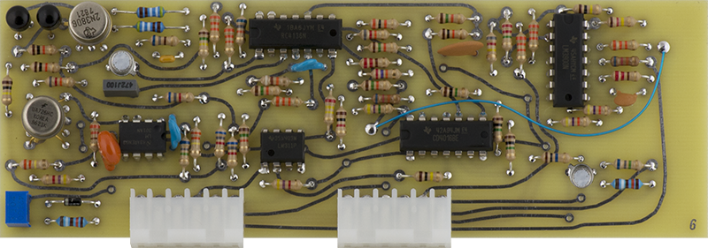
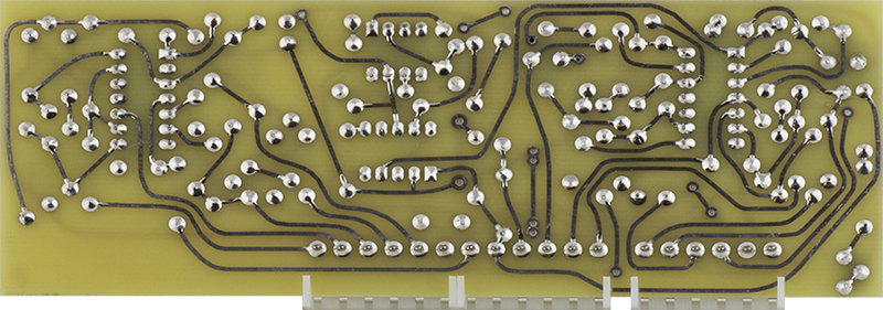
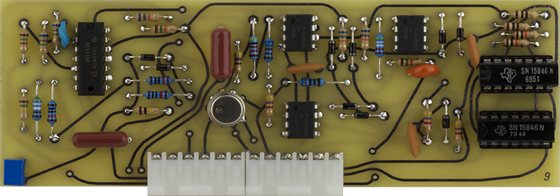
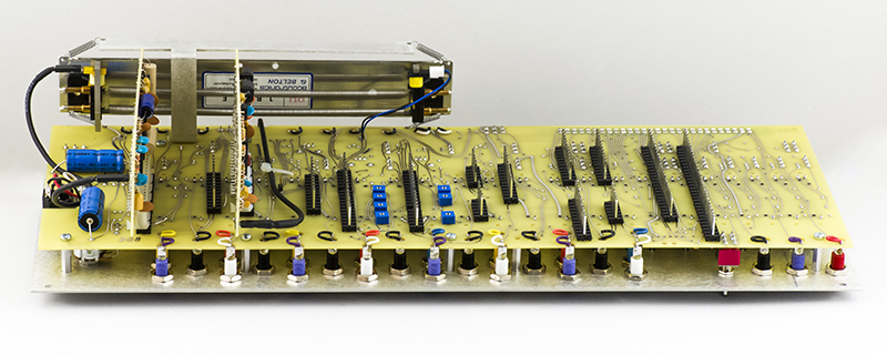
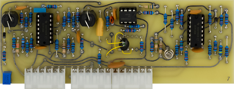
I built a V2 208 Stored Program Sound Source module for someone else. They sent me a mostly complete kit of parts (excluding knobs, slider caps and a few miscellaneous components) and I assembled and tested the module. Many of the components are sourced through Mouser but specialized parts, panel, and knobs have specific sourcing requirements. V2 is designed as per the original module with a motherboard and 12 plug-in cards. The individual cards makes the PCBs easier to assemble but it takes much longer to build them. This module took me 27.5 hours to build.
|
A scan of the manual |
|
|
A better color scan of the manual contributed by Luther R. |
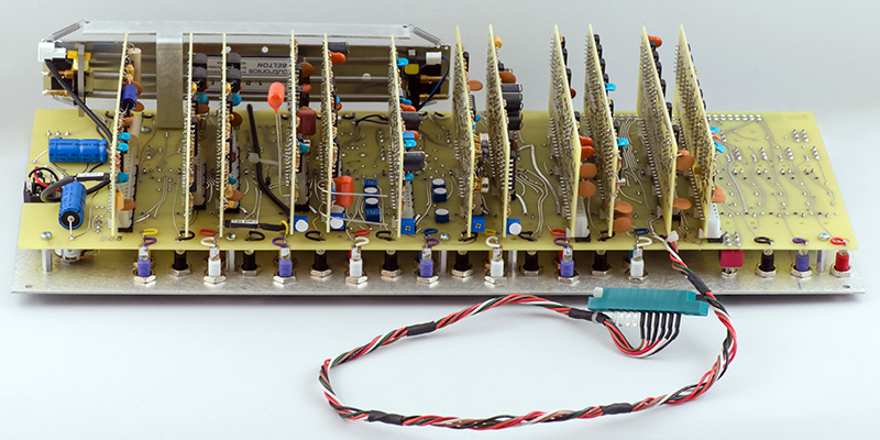
Motherboard Build Tips
According to the forum there are two wires that need to be added to the motherboard. On this version of the PCB the trace between the switches SW1 and SW8 was present but the trace between Molex 4A and Molex 3B was not so I had to add a wire on the front of the motherboard. I've been told the latest version of the motherboard now has this trace.
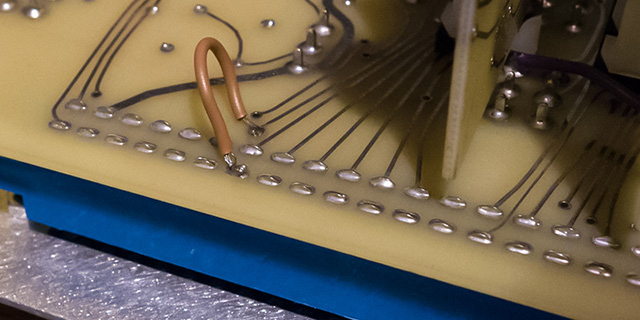
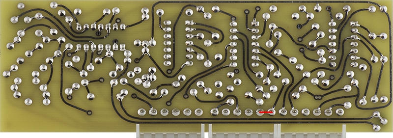
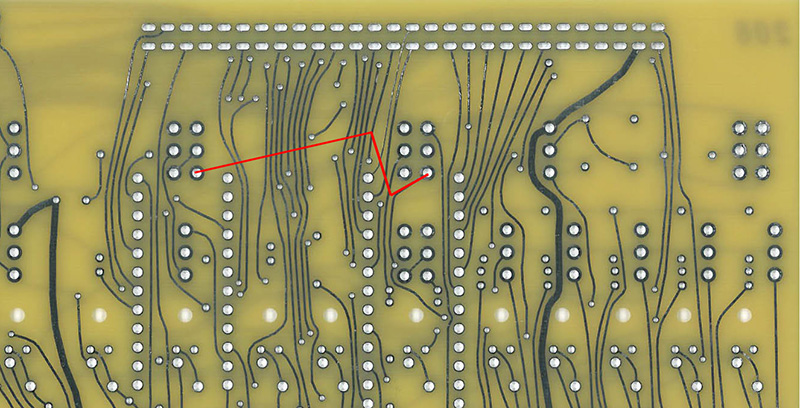
Boops on the Muffwiggler forum found there is a missing trace as the second stage doesn't trigger from the program card. Add a wire from the back from the external pin 7 of the card slot to the via just below it as shown in this photo.
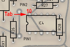
DrKorg on the Muffwiggler forum found that trimmer TR3 CO LOW FREQ TRACKING is connected to pin 11 of card 8 but should connect to pin 12 of card 8. Pin 11 is not in use so you can solder a jumper between pin 11 and pin 12 on card 8.
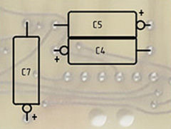
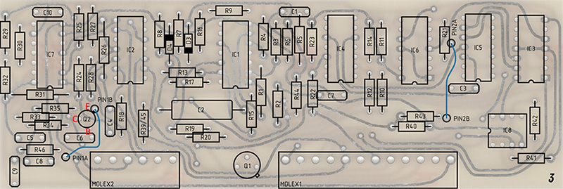
The round circle on the motherboard reference diagram indicates the capacitor + lead.
I installed the LEDs and bent the longer pin over 90 degrees to solder it to the shorter pin. These keeps the LEDs captive as I leave them unsoldered until the PCB is mounted on the panel. Then I press them through flush and solder them to a perfect height.
The switches with a nut on top of the panel only extend 16.25mm below the panel while the standoffs are 17mm long and will warp the PCB slightly. While it probably is not an issue I made a cardboard E template that I could slip under the switches and solder them 0.75mm off the PCB. I only soldered one pin then installed the top panel. I backed the nuts up against the rear of the panel and tightened the top nuts flush with the switch barrel. Then I reflowed each pin to relieve the stress and soldered the remaining pins.
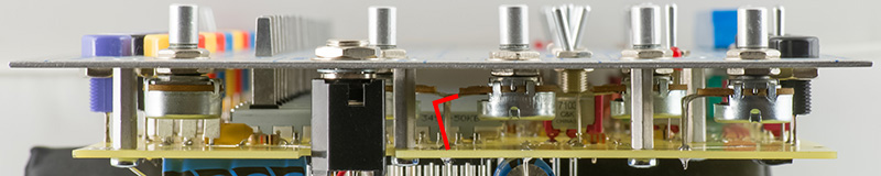
The 16mm angled potentiometers have a similar issue. I solder just the center pin so the top is just flush with the PCB. Then I backed the nuts up against the panel rear and tighten the top nuts. Then I reflowed each pin to relieve the stress and soldered the remaining pins. However when I assembled the front panel the 16mm angled potentiometers did not align very well with the front panel so the pins were bent (indicated by the red line in the center of the photo). I worried about stress fracturing the potentiometer phenolic base where the leads crimp to it as I have seen such fractures in my repairs. I rebent the leads carefully to better align with the PCB pads as can be seen in this photo.
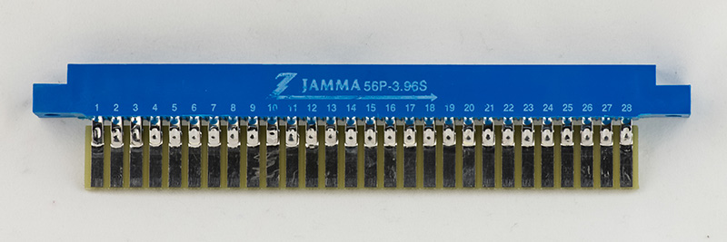
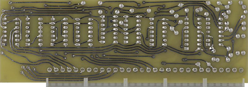
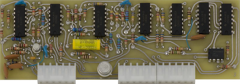
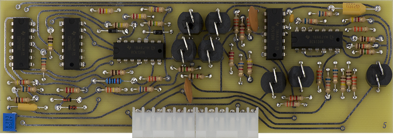
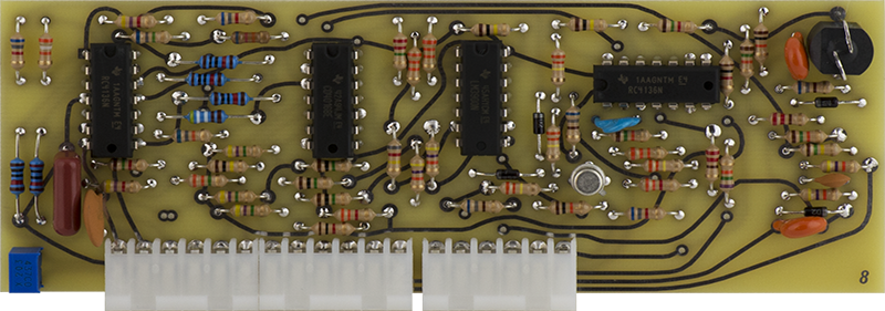
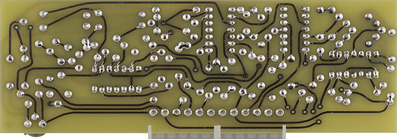
This image shows the motherboard front with the potentiometers soldered by only one pin and the LEDs unsoldered. It took 5 hours and 45 minutes to solder the motherboard. I used water washable flux solder and no-clean solder for the potentiometers, switches, and LEDs although I do clean them anyway. I used a more robust EDAC edge connector (Mouser 587-305-056-500-202) for the motherboard and used the blue Jamma 56P-3.96S connector for the front panel.
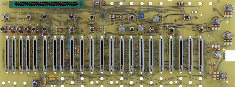
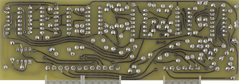
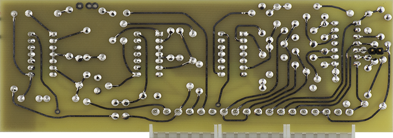
High resolution motherboard front image
Early motherboard schematic (for 208 V2 motherboard, may be some errors)
I match the wire color to the banana jack. Everything is soldered and cleaned. In total the motherboard and panel took over 9 hours to fully assemble and wire.

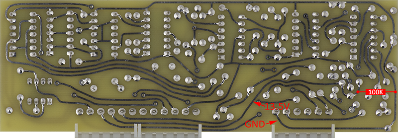
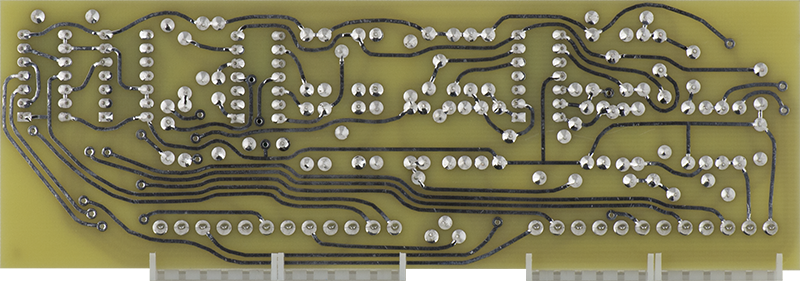
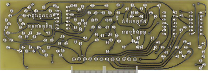
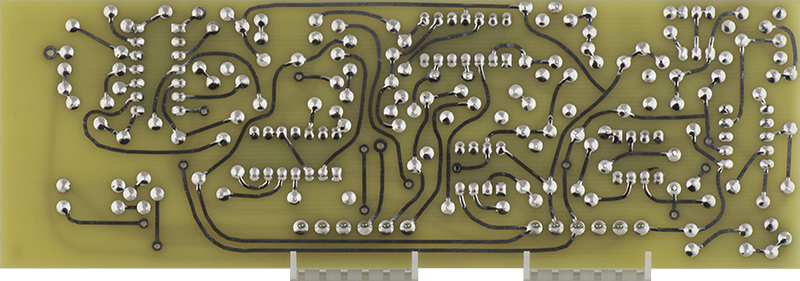
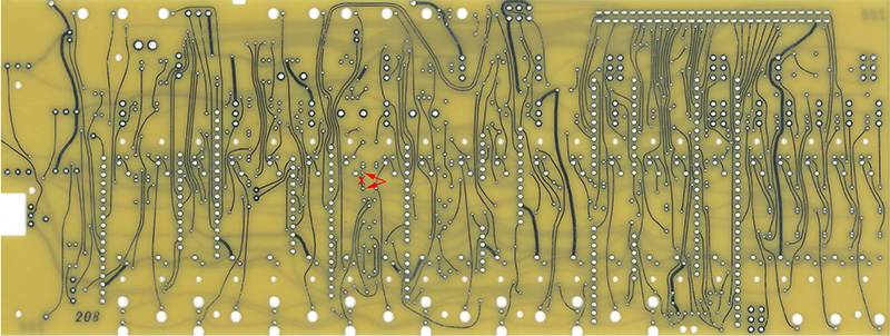
High resolution motherboard rear image
I measured the distance between the top of the front panel and the bottom of the EDAC connector and then soldered the program card extender so there would just be a small gap at the bottom of the EDAC connector. Careful soldering prevents wicking the solder on the pad. This particular connector came with blue tabs on each end that had to be cut off. The bottom of the connector sits lower than the flanges so I put two flat washers between the connector and the panel to fill the gap so the connector is firmly screwed to the panel. Total build time for the panel and motherboard was 9.5 hours.
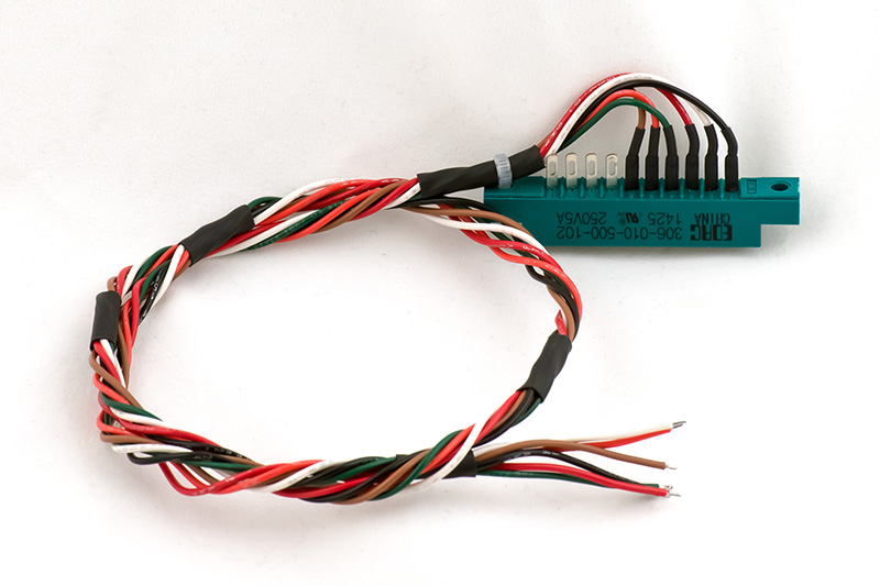
I make the power cables out of 24 AWG stranded wire and use heat shrink to hold the twist. This cable is 18" long.
Card Build Tips
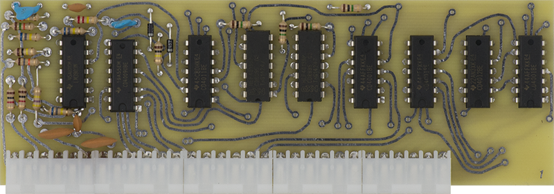
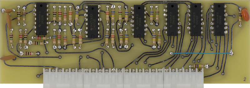
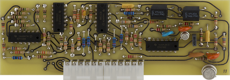
It took about 17.5 hours to build the 12 cards. Some of the simpler cards took 45 minutes while some of the more complex ones took up to 2 hours. Card 1 is the five stage sequencer and is one of the simplest cards to build.
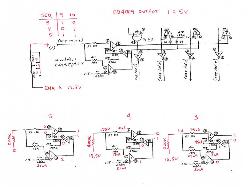
I have seen a number of issues where sequence 3 does not work properly. This analysis shows the logic of the sequencer stage select. First, decouple the ICs. Then if 3 operates as 5 then there isn't enough current from the CD4009 so decrease R9. I've not had a sequencer repair since I've done this analysis to confirm.
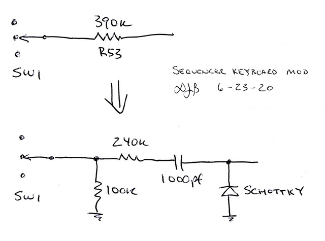
I had one 208 which wouldn't trigger properly with a 10V trigger/gate pulse. The sequencer would trigger fine but during the 5V gate portion the pulser would trigger the keyboard. It wouldn't do it on my bench until I grounded the panel to the power supply as in a boat. The issue was that the 5V gate portion coupled with the crosstalk from the pulser would trigger the comparator. I tried a number of modifications and could reliably get it to operate on the bench, but when I mounted the 208 in the boat it would misbehave. The gate portion has no function with the sequencer and since I couldn't easily troubleshoot it in the boat, I simply made the sequencer trigger AC coupled. This system used a 211 power supply which has noise issues but I was also able to get it to mis-trigger using a linear power supply. I simply replaced R53 on the motherboard with a resistor-capacitor combination. I found that a 100K termination after the switch helped to quiet the crosstalk when the switch was off and added a Schottky diode to clamp the negative excursions.
Card 2 is the random voltage source and has one wire. It also requires a cut and jumper modification.

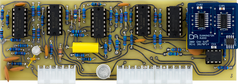
Card 3 is the envelope Generator and has two wires. I have tried to help others through email fix the 13.5V supply that is on this PCB. They tend to run a full volt over at 14.5V. The issue is the Q2 pinout is ECB, not EBC. You have to bend the leads to fit.
The regulator requires a load and the original schematics had a 100K from edge pin 4 to ground. I added the resistor on the rear.
There are sometimes issues with bleed of the EG into the audio. The LED is driven with a lot of current. There are sometimes issues with bleed of the EG into the audio. The LED is driven with a lot of current. Replace R20 with a higher value resistor. I chose 220R which cuts the current by half but the LED is still quite visible. I also added 0.1µF decoupling capacitors on the power supply pins on IC1, IC4, IC5, and IC6. This diminished the bleed in all the but the very shortest EG times. Once the Attack and Decay slider are down to .002 there is no bleed.
The EG sometimes has oscillations. The schematic shows C11 which isn't present on the card. Add a 1 nF capacitor on IC1 between pins 12 and 14.
Here is Card 3 with the Dunnington Audio Music Easel Infinite Sustain module installed. I soldered it directly to the PCB.
Card 4 is the pulser. There are sometimes issues with bleed of the pulser into the audio. The LED is driven with a lot of current. Replace R23 with a higher value resistor. I chose 220R which cuts the current by half but the LED is still quite visible. The "From Prog" typically has oscillations so add a 100 pF capacitor between IC2 pins 12 and 14.
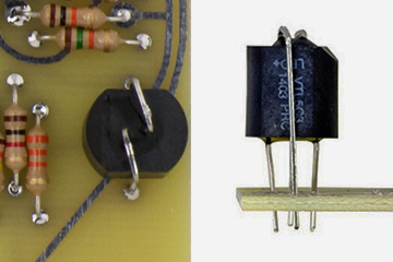
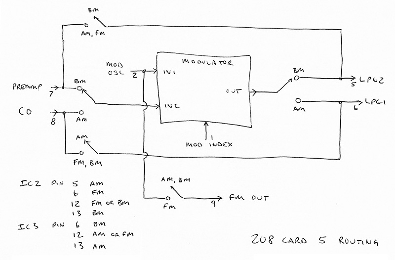
Card 5 is the balanced modulator. The + sign on the vactrol indicates the anode lead to match to the PCB reference diagram.
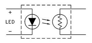
The vactrols on cards 5, 7, and 8 mount with the round resistor leads directly into the PCB and the square LED leads bent over and around into the PCB.
The BOM calls out 1N5228 for D3 and D4 which are 3.9V zener diodes. These should be 1N5236 which are 7.5V and what were used in the original design. This voltage is needed to not exceed the maximum voltage of the CD4016 parts.
There are a number of CMOS switches on card 5 that route the various signals. I made this block diagram of how everything connects. I am always a bit confused by Balance Modulator as I don't use it very often. LPG2 can select Preamp, MO, or LPG1 as its input. Selecting the Preamp Input maps this signal through LPG2 and it is modulated by the MO when Balanced Modulator is selected.
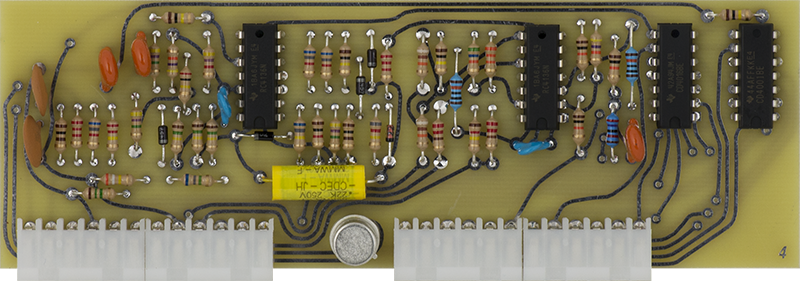
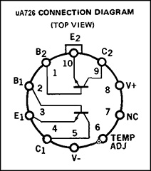
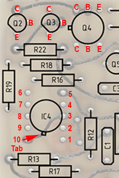
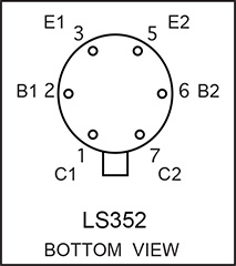
Card 6 is the modulation oscillator. The uA726 tab should point to pin 10, the oval pad on the bottom left. The LS352 tab points to Q3.
This early version CO is rather complex consisting of two COs on Cards 7, 8, and 9. Card 7 consists of the CV circuitry, Card 8 consists of the second CO and the Card 9 CO waveshaping circuitry, and Card 9 consists of the main CO. Timbre is created by using the Card 8 CO to FM modulate the Card 9 CO.
Card 7 consists of the uA720 (or equivalent) expo converter to generate an exponential control voltage for the Card 8 CO. The triangle from the Card 8 CO is added to this with a vactrol mixer to generate the exponential control voltage for the Card 9 CO. There is an additional offset trimmer TR4 (timbre) and a separate scaling trimmer TR7 (CO waveshape) for the Card 9 exponential control voltage.
The BOM specifies R3 as 1K8 while the original schematic shows 10K. Increasing R3 to 10K significantly increases the timbre folding. I ended up selecting R3 to be 8K2 for best performance.
The reference designator for the uA726 shows pin 1 so the tab should point to pin 10 on the upper left.
Card 8 is the second of three cards and consists of a second CO and the waveshaping circuitry for the main Card 9 CO. The CO is a typical triangle integrator. The exponential control voltage is converted to a negative control current for the integrator. The comparator then adds in a positive 2X control current to reverse the triangle. The square wave output, along with a pulse derivative, is used for the Card 9 CO waveshaping circuitry.
Sometimes the non-sine waveforms have oscillations. Add a 100 pF on IC4 between pins 12 and 14.
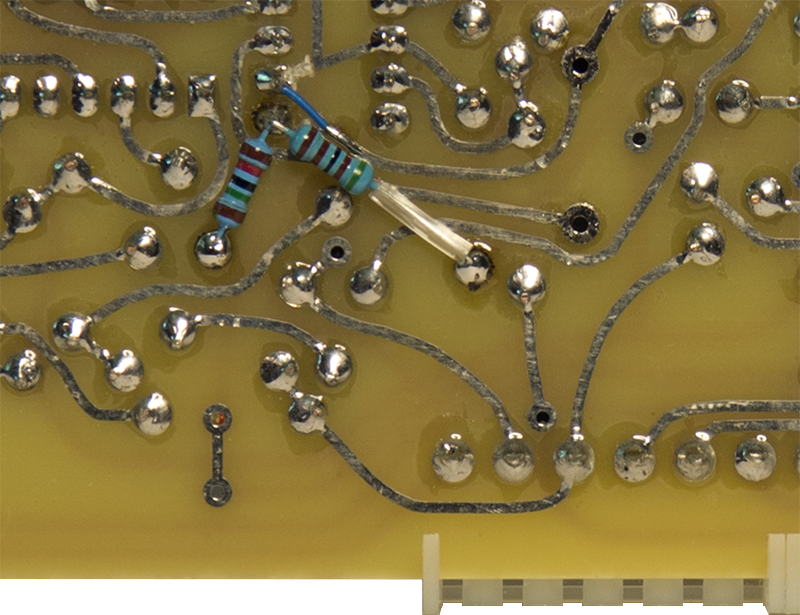
TR3 on the motherboard connects to pin 11 of card 8, not pin 12. Simply short pins 11 and 12 as shown in the photo to fix.
I helped an individual who had a glitch on the sine. Normally this glitch is the inverted triangle and is symmetrical on both the positive and negative peak. In his case it was only on the positive peak which is inverted from the output of card 8. We examined the triangle input and the sine output from the sine shaper circuit and the triangle looked perfect and the sine had this glitch on the negative peak only. IC2 is operated on +15V and -3.4V as determined by R56 and R57 so it can operate with the bipolar sine input on pin 8. He had used a CD4066 but changing to the CD4016 eliminated the glitch.
The TI datasheet shows a maximum supply voltage of 20V but the Fairchild datasheet only shows a maximum supply of 18V and this is operating at 18.5V. I don't know if it is related to that, or perhaps crosstalk from the square or pulse input. This resistor divider for the negative supply has an equivalent series resistance of 770R which is quite high and could lead to operational issues.
Card 9 is the third of three cards for the complex oscillator and is a the main thru-zero CO. Similar to Card 8, the exponential control voltage is converted to a negative control current for the integrator. A positive 2X control current is switched in to reverse the triangle. The control for this switching is a SR flip-flop with steering logic controlled by a comparator that detects the sign of the exponential control voltage. This reverses the control current for the thru-zero operation.
A complex comparator circuit is used to set the triangle minimum and maximum triangle voltage consisting of a sample and hold, a full wave rectifier, a summing amplifier, and a minimum and maximum comparator. The Card 8 CO square wave is differentiated and the falling edge is used to sample the Card 9 CO triangle. This resulting voltage is offset by a full wave rectification of the exponential control voltage and used to adjust the set points of the minimum and maximum comparators, thus adjusting the amplitude of the Card 9 triangle so the frequency matches the Card 8 CO frequency. The sampled triangle is available on TP1 and the offset control voltage is available on TP2. R5 on Card 9 adjusts the scaling of the offset control voltage to help maintain stability between the two oscillators.
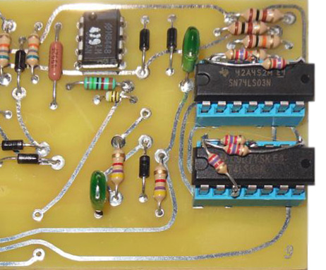
I used sockets for the rare 846 DTL ICs. The tab on the DG200 points to the square pad and pin 7 needs to be cut off to fit the PCB.
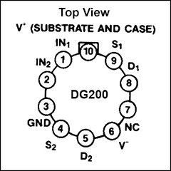
The MC846 is hard to find and is a DTL quad nand gate with resistor pullups on the outputs. This allows the outputs to be tied together for a logical AND function. You can substitute a 74LS03 which has open collector outputs but you have to add external pullup resistors. This is a generic replacement for a MC846. I chose 10K pullups. You can add them on the top of the part.
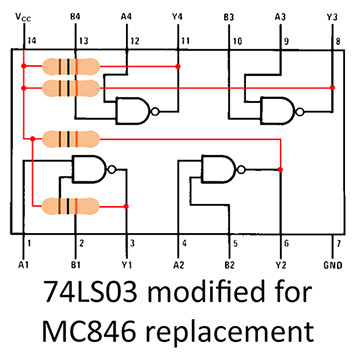
Several outputs are tied together in the actual circuit so you don't need to add all eight pullup resistors. This schematic shows which resistors are needed.
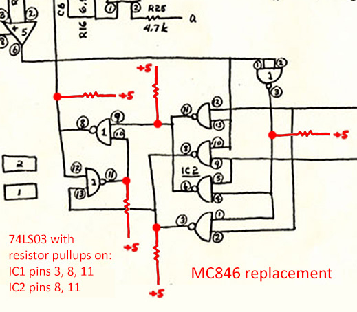
DonT verified this circuit using 2K7 pullups and posted his results on Muffwiggler. This is his photo of his modification.
Card 10 is gate 1 and the preamp. I used square pins for the preamp input connector. I used RG174/U coax from the preamp jack to a 2 pin FCI header to mate with the square pins. The preamp input is routed to the output by the the Signal Routing switch in the up position through LPG2. When the Modulation Switch is in Balanced External then the Modulation Oscillator will modulate it as controlled by the Modulation Index slider.
Card 11 is gate 2.
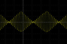
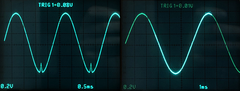
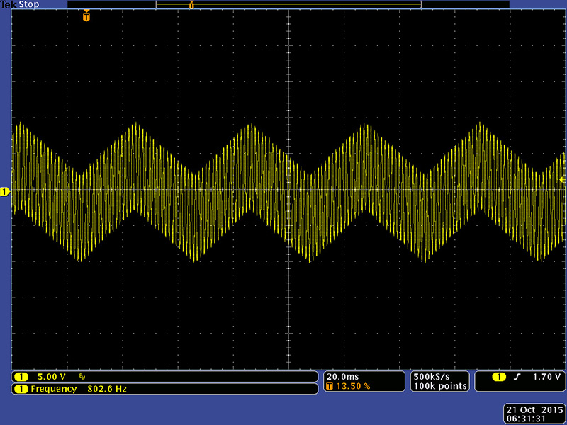
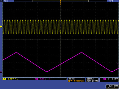
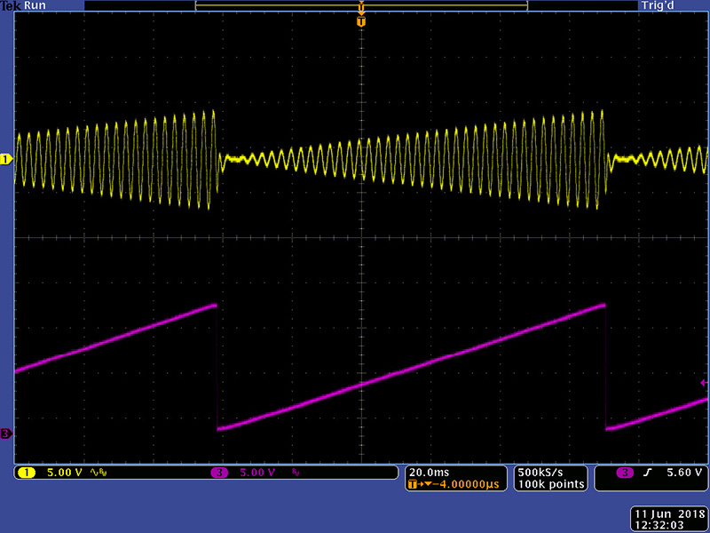
I recently repaired a 208 where the MO was not functional. I was monitoring the MO in the signal output and once I got it working the output was very weak. Looking at it on an oscilloscope the output was highly differentiated. The MO is mixed to the signal output through C4 on Card 11. This is a 1 µF capacitor feeding a 10K potentiometer which is a high pass filter with a lower frequency cutoff of 15 Hz. I increased C4 to 47 µF with a capacitor on the rear of the card where there is more room. This allows lower frequency MO output to be passed through on the signal outputs. This scope image shows the mixing of a low frequency MO triangle with a high frequency CO which is not possible with the original 1µF capacitor.
Card 12 is the reverb driver and output. C2 is a specified as 390 µF which is a value that was available years ago. Today's standard values are 330 µF and 470 µF so I used a 330 µF instead of buying a NOS capacitor. The LM380s can break into high frequency oscillation quite easily. Typically it is a wrong value component but on one that I repaired it was leakage through FLUX! Cleaning the PCB was sufficient to stop the oscillations. When one of these oscillates, it can ripple through the whole system so it is hard to find the cause and effect. Clean your boards!
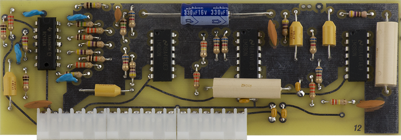
Card 8 has coax wiring from the Preamp jack and I chose to run the reverb return direct with shielded wire. I cut the trace from pin 5 on IC1 and added square pins on the rear so I could connect with an FCI connector. IC1 pin 5 is the input to the reverb recovery amp and the outside trace (far right on the PCB rear image above) is ground. You can use a 0.100" MTA connector to mate directly with the reverb tank (image below)
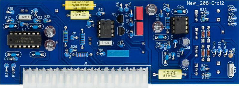
The reverb circuitry on Card 12 is not the best. I chose to build the Boops Card12 Replacement.
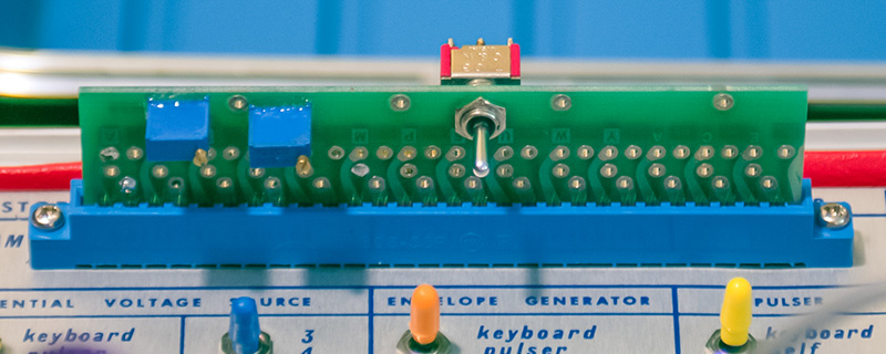
Program Card Connector
Don used the number/letter designation for the program connector on his schematics. I can never remember the letter sequence (since letters are missing) and which is the letter side and number side and do they start on the left or right. I made this Program Connector document with appropriate signal names. I used "trigger" instead of "pulse" to differentiate it from Pulser so I didn't have Pulser pulse out, etc. I also added the few differences from the BEMI connector that I know of.
208 Program Board Connector Pin Definitions
Modifications
I started verification first with the pulser and sequencer and immediately ran into a problem. The sequencer would operate correctly in the 3 stage mode but not 4 or 5. Sometimes 4 stages would operate correctly and other times it would also operate as 3. Set to 5 stages it would sometimes operate as 3 and sometimes it would skip stage 4 or stage 4 and 5 would come on simultaneously. I found postings of others with similar problems with a variety of fixes suggested. I found that putting scope probes on various parts would correct the issue. On the 1973 schematics there are 1M resistors in series with the D inputs to the four CD4013 flip-flops. Their purpose is to slow down the D inputs and I suspect modern CD4013s are faster. I suspected a race condition but couldn't find it since putting my scope probe on a number of pins would correct it. Adding a bit of capacitance on various pins would correct it so I decided to add a 51 pF capacitor on the clock from IC1 pin 4 to +15V. Adding the capacitor to Q (quiet ground) also worked but there is only N (noisy ground) on this card which didn't work. I didn't debug it any further since I am building this module for a customer.
On subsequent repair jobs, I have had two 208s that would sequence 2, 4, or 5 steps. They would not operate correctly at 3. If you look at the original 1973 schematics IC8 is used to enable or disable stages 3, 4, or 5 as selected by the logic of IC1. IC1 pins 9 and 10 are logic outputs and should be 01, 10, 11 for the three selections. D1 and D2 OR the two bits for stage three. For some reason, the selection logic is 00, 10, 11 instead. Since these were repairs with an hourly charge rate I did not investigate to root cause. Stage 3 should always operate but it appears this logic was designed for 2, 3, 4, or 5 stages but only 3, 4, and 5 are used. I simply corrected the issue by lifting IC8 pin 9 and connecting it high so stage 3 is always enabled. Note that although the front panel switch does not enable a 2 step sequence the program card can be set for this. This modification eliminates that possibility.
I could not tune the Complex Oscillator. A 1.2V increase in keyboard CV would only increase the pitch by 1.6X, way short of an octave. I decreased Card 7 R14 from 120K to 75K to tune it to 1.2V/Oct. You can lower this to 68K for 1V/Oct and there is enough range in the trimmer to adjust also to 1.2V/Oct.
The frequency range was 17 Hz to 2.5 KHz which is 6 octaves but a fairly low frequency. I changed Card 8 C1 and Card 9 C3 from 15 nF to 5.6 nF which shifted the range to 50 Hz to 6 KHz. I personally would like a little more low frequency so would recommend a 7.5 nF Mouser 667-ECW-H8752HV capacitor for a range of 35 Hz to 5 KHz, or C1 to E8, where C4=middle C. The owner was happy with the 17 Hz to 2 KHz range since it matches the slider legend so I left the original capacitors installed.
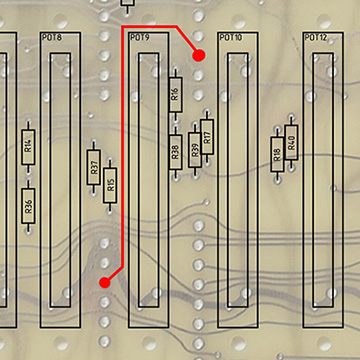
On a recent repair the CO coarse slider useful range was only about the first half travel. I cut the trace on the motherboard and added a series resistor in series with R45 to reduce the gain of the CO coarse slider. You can cut a trace on the rear of the motherboard at the X and jumper a resistor between the pad and feed through (marked by arrows). I determined the resistance to add empirically. Large motherboard image
Likewise the Modulation Oscillator would not tune either so I decreased Card 6 R5 from 190K to 82K to tune it to 1.2V/Oct. I adjusted the MO Offset so 16 Hz mapped to the slider legend with the fine pitch control centered. There is typically enough range that you can also tune to 1V/Oct.
On some modules I have repaired the MO range is way too low. Increase R9 on card 6 to raise the frequency. Determine the value empirically although the last value I used was 330K.
On some units I have repaired Timbre would decrease as the CO frequency increased. I lowered R46 on Card 7 which increases the Timbre modulation amplitude. In some cases I dropped this from 15K down to 1K. I assume this is due to variation in VT2. Later I discovered that R3 on Card 7 is 1K8 and the original schematics show it as 10K. I ended up selecting an 8K2 for R3 on my unit. I don't know if this would affect the timbre decrease with increasing frequency.
There are also sometimes issues with bleed of the EG into the audio. The LED is driven with a lot of current. You can increase the value of R20. I chose 220r which cuts the current in half. I also added 0.1µF decoupling capacitors on the power supply pins on IC1, IC4, IC5, and IC6. This quieted the bleed in all the but the very shorted EG times. Once the Attack and Decay slider are down to .002 there is no bleed.
There are sometimes issues with bleed of the pulser into the audio. The LED is driven with a lot of current. Cut the run to the edge pin 8 and solder a 1K resistor across the cut. This will drop the current significantly but the LED is still quite visible.
I cut the run on Card 12 to IC1 pin 5 and ran a coax cable directly from the reverb output to IC5 pin 1. Ground is on a nearby trace. The reverb on these is pretty muddy. I cut the trace on Card 12 to edge pin 12 and added a 15K resistor. This keeps some dry signal present when the reverb control is turned fully CW.
The pinout for Q2 on card 3is ECB, not EBC as described above. Also add a 100K load resistor as shown above.
Add a wire from the back from the external pin 7 of the card slot to the via just below it as described above.
Cut and jumper the trace on Card 2 as described above.
Solder a jumper between pin 11 and pin 12 on card 8 to fix TR3 CO LOW FREQ TRACKING.
Optionally increase C4 on card 11 to 47 µF for lower frequency MO mix on the signal output.
The reverb on these 208s is really muddy (IMHO) and only about the first 30% of the control is usable. I helped someone via email change the feel of this potentiometer by adding a resistor between the wiper and the CCW pin (towards the center of the PCB) to change the potentiometer feel to log. Use a value 1/10 of the potentiometer, so 4K7 for 50K and 10K for 100K.
You can decrease the sensitivity of the Fine Tuning potentiometers by increasing the value of R78 and R74 on the motherboard.The tab closest to the pins on the CO fine and Waveshape potentiometers can short to the -15V run underneath. Break this tab off before soldering. If your 208 is already built, then you can desolder these controls from the rear, and pull them off the board. I raise them until the pins are flush with the PCB and then resolder.
The headphones are coupled with 470 µF capacitors. These capacitors can retain a charge with no headphone connected and when inserting a plug can result in a loud "pop". Simply put a 10K resistor from each terminal to ground on the headphone jack. This modification is included in the Portabellabz boards.
A trigger/gate pulse would not reliably trigger the sequencer. The pulser would trigger the sequencer during the gate portion of the pulse. I ended up AC coupling the trigger to the sequencer. See the modification described above in the Card1 description for details.
A 218 V1 will sometimes not trigger correctly as the pulse output is only about 6V. You can parallel a 240K resistor across R56 on the back of the motherboard to change the pulse in threshold from 10V to 5V. This changes the threshold for the Pulser, Sequencer, and Envelope Generator. However, the Pulse input will NOT trigger the pulser when Keyboard is selected. There is a run missing to SW10. Add a wire on the motherboard rear between SW8 and SW10 as shown below.
Card 5 Modifications
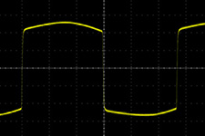
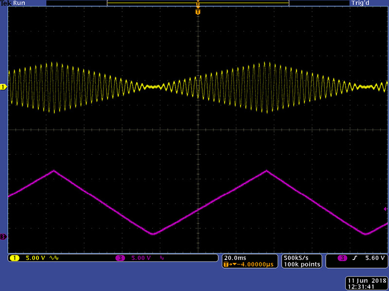
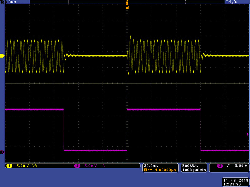
I've never liked how card 5 worked. Typically there is a level change when selecting AM modulation, even with the index at 0%. This is due to the AM switching in a completely different circuit. I adjusted R29 to balance the dry level for AM to be the same as on FM with the index at 0% The left image is the CO and MO on FM with the Index at 0% and the right image is when AM is selected.

Trimmer R18 sets the balance between the vactrols used in the modulator for 100%. It is best set by looking at the signal at pin 8 of IC4. The signal levels between the three MO waveforms are different so you have to pick one to adjust to 100% modulation. I choose the triangle waveform. The modulator always runs at 100% modulation. The wet output is inverted with a gain of 2X. Increasing output corresponds with increasing positive MO.
Index works by crossfading the wet and dry signals using VT6 and VT7. Near mid index the wet-dry signals are equal. The wet and dry signals will cancel at maximum CO which occurs at the maximum MO signal. Increasing output corresponds with an increasing negative MO.
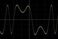
At 100% index there is no dry signal so you have only the 100% modulated CO at 2X gain. Increasing output corresponds with an increasing positive MO. I find this confusing and non-intuitive. Here is a scope image of the various Index settings. At maximum Index the CO is very hot and corresponds to the AM waveshape. At 30% index the CO corresponds to an inverted MO.
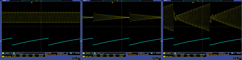
No AM Index 0.3 AM Index Max AM Index
I want the Index control to AM modulate between 0 and 100% as per the panel legends. I changed IC4C from an inverting to non-inverting configuration and set the gain so the peak level was the same as the dry signal. Cut the runs on the back of the PCB to IC4 pins 8 and 9 and jumper the run going to pin 8 over to pin 9, remove R23, add a 15K resistor from pin 10 to pin 8 and add a resistor from pin 8 to ground to set the proper gain (I've used values between 5K and 10K).
The result is 0 to 100% modulation using the Index slider.
uA726 Modifications
For my personal 208 I chose to not use uA726s even though I have some. Instead I matched NPN transistor pairs on my Tektronix 577 curve tracer and bonded them together with a 3300 PPM/C 330R tempco (R12 on card 6 and R26 on card 7). An easier way to do it is to simply buy tape and reel. Then you can bend the leads a bit, put some epoxy on the faces, and tape them together with the tape and reel.
The tempcos are Panasonic ERAS33J series from Mouser (667-ERA-S33J331V). Their specifications aren't the best as the resistance has a +/-5% value tolerance and the temperature coefficient has a +/-10% tolerance over temperature. I tape cardboard to the PCB and tape the leaded tempco so I can epoxy it to the top of the NPN pair.
I installed the 208 in a boat and powered it up in the garage with an ambient temperature of 62.2°F. I monitored the CO frequency and it stabilized pretty well after 22 minutes so I called this the initial frequency. I monitored the case temperature of the boat and the frequency for the next 2 hours. After one hour I powered down the 208, moved it into my studio, and powered it back up for the last hour. The total drift over a temperature change of 8.8 °F was -5.43 cents. I have no idea how this compares to a non-tempco version or a uA726 version but it is good enough for my studio needs. The gray background cells indicate the warm up time. If you have measured the temperature stability with a uA726 or a matched pair without a tempco please contact me with your data.
|
208 Complex Oscillator using 2N3904 matched pairs with 330R Panasonic ERAS33J series tempco |
|||||
| Time in minutes | Ambient temp °F | Boat case temp F | CO Freq Hz | Delta Hz | Delta cents |
| 0 | 62.2 | 66.2 | 1044.5 | Turn on | |
| 3 | 62.2 | 66.9 | 1003.8 | -40.7 | |
| 5 | 62.2 | 67.3 | 1003.3 | -0.5 | |
| 12 | 62.2 | 68.5 | 997.8 | -5.5 | |
| 22 | 62.2 | 70.8 | 996.2 | 22 min warm up | 0.00 |
| 37 | 62.2 | 72.8 | 995.1 | 1.1 | -1.33 |
| 50 | 62.2 | 73.0 | 994.5 | 1.7 | -2.05 |
| 62 | 62.2 | 74.0 | 994.1 | 2.1 | -2.53 |
| 90 | 62.2 | 75.2 | 993.3 | 2.9 | -3.50 |
|
Powered down, moved inside, powered up |
|||||
| 90 | 71.0 | 76.0 | 994.9 | 1.3 | -1.57 |
| 110 | 71.0 | 77.0 | 992.8 | 3.4 | -4.10 |
| 125 | 71.0 | 77.7 | 992.2 | 4.0 | -4.83 |
| 127 | 71.0 | 78.2 | 992.0 | 4.2 | -5.07 |
| 142 | 71.0 | 78.2 | 992.0 | 4.2 | -5.07 |
| 150 | 71.0 | 78.2 | 991.7 | 4.5 | -5.43 |
Initial Power On
I get asked a lot about how to power-on a 208. I decided to quickly summarize my approach. I do all of this verification with an oscilloscope.
I do an extensive visual inspection of every component and all the runs on the motherboard checking for value and orientation of the LEDs. I especially look for unsoldered edge pins and solder bridges. Sometimes the edge pins don't wet and are hard to see but if I see a darker area around the pin where the solder is convex instead of concave I resolder. The runs and pins are large so you can use a reasonable amount of heat. I fully assemble and wire the motherboard to the panel. I always use stranded wire for the bananas (1.125") and 3.5mm (1.25"). I also color coordinate the wire to the banana. The reason I don't wire straight across is because if you have to do a future repair, you can generally lift the panel enough without unsoldering all the wires.
I generally verify with a scope on the edge connector pins. I start with just card3. I verify continuity from my power supply to the ower pins on an IC to verify the power cable is connected. Then I power it up and edge pin 4 (the reverb side is pin 1) should have 13.5V on it. Nothing will operate if this voltage isn't high. Sometimes the circuitry doesn't work right and the voltage is higher. It will still function but is not operating correctly.
I then install cards 1,2, and 4. I start with card 4 to verify the pulser is working. Then I use the pulser to clock the sequencer, random, and envelope. The sequencer will not always work correctly unless you have added the decoupling capacitors.
Once I verify these I add card 6 and verify the MO on edge pin 4. You can also verify the MO CV on the upper right banana connector.
Once that works I add cards 7-9 and verify the CO. There are two COs and at this point I don't worry about some abnormalities as they haven't been calibrated. The secondary CO has a triangle waveform on card 8 pin 15 and a square wave on pin 14. The primary CO has a triangle wave on card 8 edge pin 9. The wave shaping outputs are on card 8 edge pin 4. I look for basic functionality as it is not calibrated.
Then I install card 5. The FM almost always works as that just patches CV over to the CO. The modulator outputs are card 5 edge pins 5 & 6. Again I just verify basic functionality of AM. I don't worry about the Balanced Mod yet as it uses the same circuitry.
Then I install cards 10-12. Without the reverb tank connected the recover op-amp is at the rail so I short out the reverb return input on the motherboard. Once these cards are verified I install the reverb tank and verify functionality.
Then I modify, calibrate and fine tune the 208.
Calibration
Here is my trimmer descriptions and the procedure I used to calibrate the module. Some trimmers had very little effect so I just centered them.
| Trimmer | Function | Procedure |
| MB front TR1 | MO Tuning | Set to center and adjust as needed to trim after setting MO Range. |
| MB front TR2 | CO Tuning | Set to center and adjust as needed to trim after setting CO Range. |
| MB rear TR3 | CO LF Lin | I found little tracking effect so set to center. There is an error on the motherboard. See card 8 description above to correct. |
|
MB rear TR4 |
Timbre | Set Timbre to max, Card 9 R5 to center, then view sine wave output on scope and and
adjust TR4 for symmetrical folds in waveshape.
|
| MB rear TR5 | CO Offset | Adjusted to 100 Hz with front panel slider at bottom. |
| MB rear TR6 | MO Offset | Adjusted to 16 Hz with front panel slider on 16. |
|
|
||
| MB rear TR7 | CO Waveshape | Set waveshape to square wave and adjust for symmetrical
top and bottom.
|
| MB rear TR8 | CO Range | Set to 1.2V/Octave. |
| MB rear TR9 | MO Range | Set to 1.2V/Octave. |
| Card 5 R18 | CO AM Symmetry |
Set MO Index until 100% modulation and adjust for symmetrical AM modulation. I found that it was not symmetrical on all waveforms so set it for the triangle waveform.
|
| Card 6 R51 |
MO High Freq Tracking |
I found little tracking effect so set to center. |
| Card 7 R45 |
CO High Freq Tracking |
I found little tracking effect so set to center. |
| Card 8 R42 | CO Sine Shape | Adjust for proper shaped sine wave. |
R5 is the low frequency adjustment for the CO on card 9. Sometimes at low frequencies the two COs do not track and it can be heard as instability in frequency. |
||
| Card 9 R5 |
CO Low Freq Track |
Adjust for stable oscillation with the frequency control set to minimum. Sometimes it takes some further adjustments to CO Waveshape so recheck and iterate between the two as necessary. |

Here is the module nearly done. You can see the two timing capacitors temporarily installed on cards 8 and 9. I haven't yet decided what values to leave in the module. You can also see the white dots over the trimmers I install when complete as it makes it less error prone to adjust the wrong trimmer.
iProgram Card
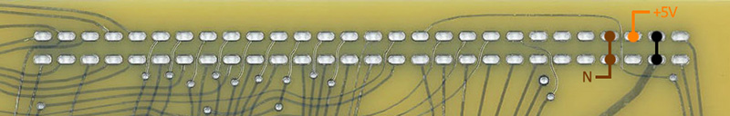
The iProgram card requires power connections that aren't on the V2 or V2.1 program connector. You have to add both +5V and ground. The Q ground is on pin 2 but needs to be on pin B. The N ground needs to be on pins 4 and D. +5V needs to be on pin C. The Q and N are connected together on card 12 so you can simply jumper pin 2 to pin 4, B, and D. Note the connector numbering may be numbered different than the PCB and these are different than BEMI. Use this rear photo of the connector as your guide. There is also information on the iProgram card & 208r rev2? thread on Muffwiggler
V2.1
I built a black version of V2.1. While most information is the same, I did create a separate page for it here.
Program Card
I wanted a modulation oscillator octave switch but dislike drilling an extra hole in the panel. Another alternative is to remove the violet Pressure jack under the modulation oscillator frequency slider and use that location for a switch. I chose to make a custom program board which allows a None / 1 Octave / 2 Octave selection. I just repurposed another PCB which had the correct edge fingers, cut it off at the correct length, and wired it up. It works great.
MO Octave Switch schematic (for 2V/Octave MO)