|
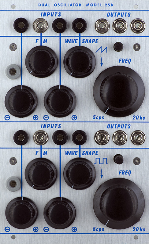
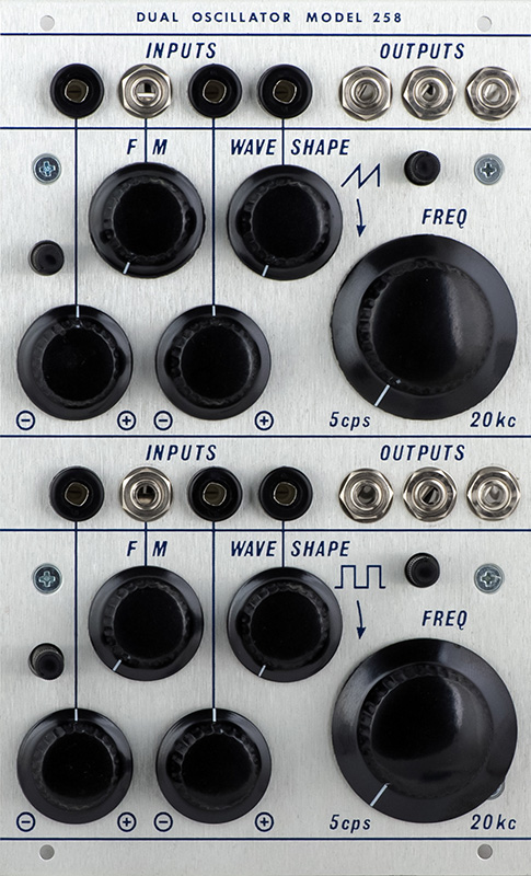
258 Dual Oscillator Module |
|
V1
I built a V1 PCB set after the V2 and V3. V1 is designed for LM741 op-amps, uA726 expo pairs, and a number of vintage transistors. I chose to build this with TL071 op-amps, a matched pair of 2N3904 with a 1K tempco, and all 2N3904/6 transistors. I used cut tape for the transistors so did not match the expo pair. I used a 1K tempco so had to modify the CV gain appropriately and I left out the high frequency compensation parts.
The trimmers aren't labeled as to function. TR6 on PCB1 is the V/Oct trimmer. On PCB2 TR1 is high frequency, TR2 is offset, TR3 is sine shape, and TR4 and TR5 are the waveshape trimmers.
Epilog
After building the MEMS 258 I built another 258 V1 using that style front panel with my MEMS modifications so the three CV inputs match.
You can see the 20 turn trimmers for the scale adjustment on the rear. I used all 2N3904 and 2N3906 transistors including the expo pair.
I hand tweaked the sine and waveshape resistors to produce some really nice waveforms.
V2
I've repaired and calibrated a number of 258 V2 Dual Oscillator modules. Some track, some do not and I've never understood why. I decided to build one for myself and dive deeper into the circuitry. I wanted to experiment with the difference between the discrete current source and an op-amp current source.
I used tape and reel 2N3904s for the differential pair. I epoxied them together and soldered them in place of the uA726. I was going to use a 150R SMT tempco for R33 and R89 mounted on top of the pair but decided to change resistor values so I could use a 1K axial tempco instead because of the better specifications.
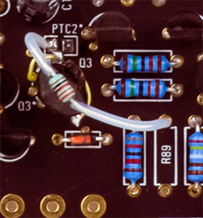
With the high frequency trim (Linearity) removed I was able to get 6 octaves of range at 1V/Oct CV. I was surprised I didn't need a high frequency trim. The discrete current source didn't seem to be an issue either. I experimented with an op-amp current source but it didn't change things appreciably.
|
258 V2 Modifications VCO 1
VCO2
|
|
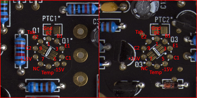
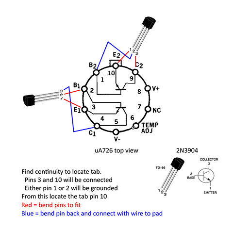
* * * REV2.0 WARNING * * * My black Rev 2.0 PCB (shown above) has pins 5 and 8 swapped (reverses +15V and -15V) and pins 6 and 7 swapped (reverses the temp adj and NC). I didn't use these pins so it doesn't matter but you don't want to solder a uA726 without lifting and swapping pins 5 and 8 and bridging pins 6 and 7.
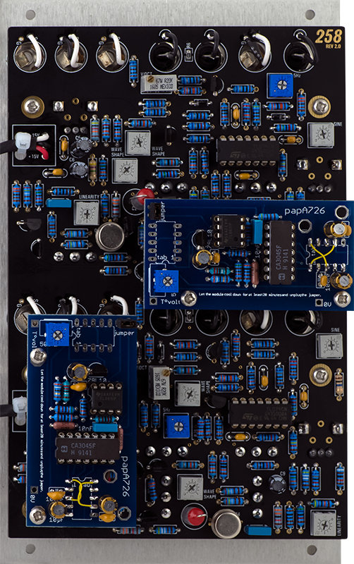
Next is another V2 I built with the Portabellabz 208 pA726 adapter boards (shown below) which did work. In the 258 pin 1 is ground so that is jumpered to pin 7. I don't remember why pins 3 and 7 are jumpered since they should be connected on the PCB. I can only think of two reasons why this worked: (1) I mounted the PCBs with screws and hand wired the pins. I might have checked continuity and wired them accordingly, or (2) there are different versions of Rev 2.0 PCBs.
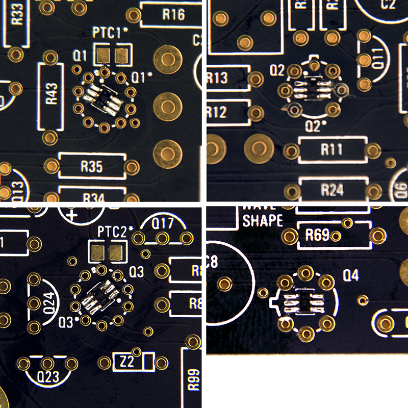
Now to add more confusion I found this reference diagram I made from the Rev 2.0 PCB for yet a different build. Note the pinout is correct, but exactly backwards so you would install the uA726 from the rear. I would have made this diagram by checking continuity.
My only conclusion is there must be multiple versions of Rev 2.0, which isn't surprising. You need to verify the pinout of the Rev 2.0 uA726 before building! |
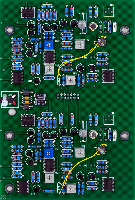
This is a 258 I built for a customer that uses two of the Portabellabz 208 pA726 adapter boards. I had to drill three holes and jumper one trace that was in the way to mount them so no trimmers were covered. The two yellow wires on the adapters eliminate the need to run two additional wires between the PCBs.
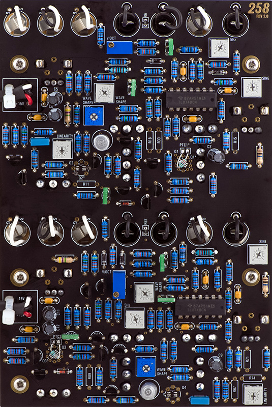
This is a V2 I built for a customer using the SMT dual pairs. They are hand solderable if care is taken.
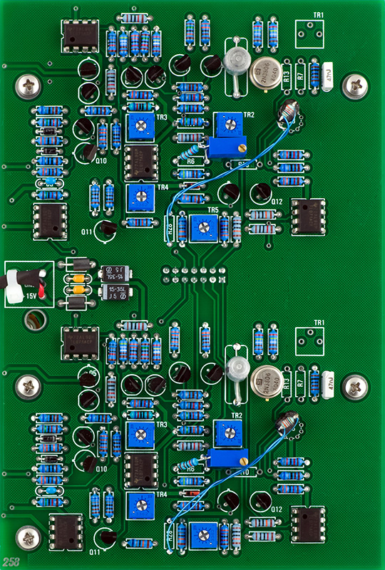
This is a photo of the final build. I modified the resistor values described above to use a 1K 1/6W tempco which I mounted on top of the dual NPN with thermal grease. I did not install the high frequency trim components (except for the trimmer since it has to be soldered from the rear). Both VCOs tracks well over 4 octaves without these components. I also used SMT adapters for the J201 transistors. These are designed specifically for J201s for a GSD pinout. I changed the SMT resistors to 110K to track 1.2V/Oct, lowered R40 and R96 to better tweak the sine shape, and increased R21 and R77 to drop the maximum frequency with the coarse control to just over 20 KHz. I have gone as low as a wire link for R40 and R96. Sometimes this increases the amplitude of the sine which can be tweaked with R37 and R93.
V3
I built a 258 V3 Dual Oscillator module for someone else. They sent me a mostly complete kit of parts and I assembled and tested the module. Many of the components are sourced through Mouser but specialized parts, panel, and knobs have specific sourcing requirements.
The V3 includes a CA3046 transistor array which is used for the exponential pair along with a heater to operate at 55°C junction temperature. Each oscillator is separate on the PCB including the power supply connections. I chose to use a single edge connector with two power cables to the module.
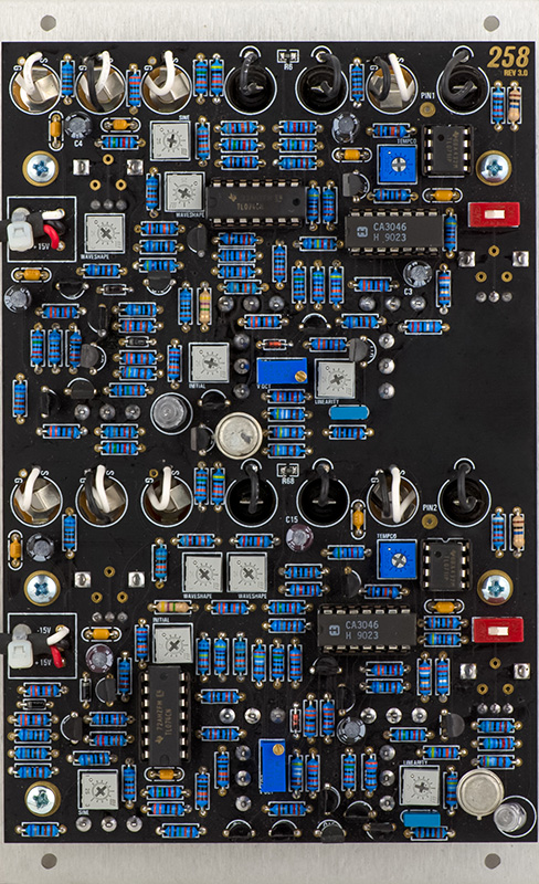
I made a reference diagram from the PCB.
Operation
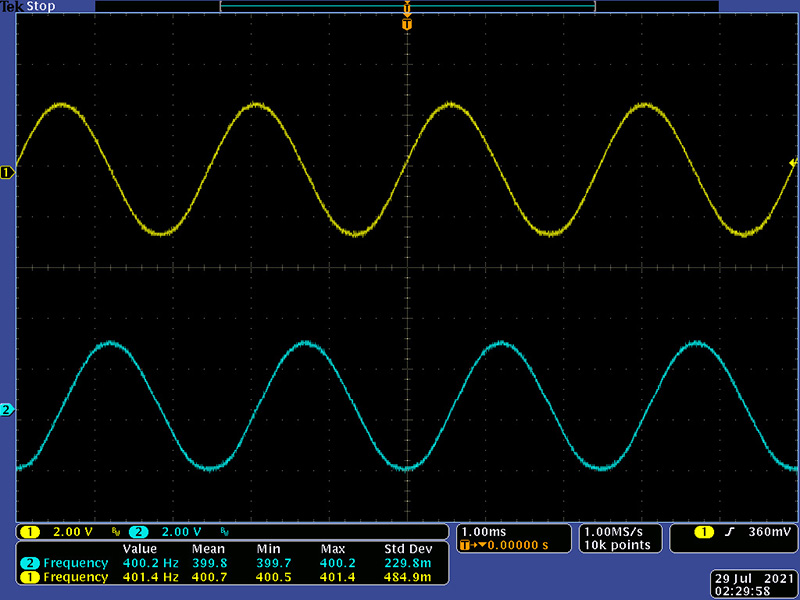
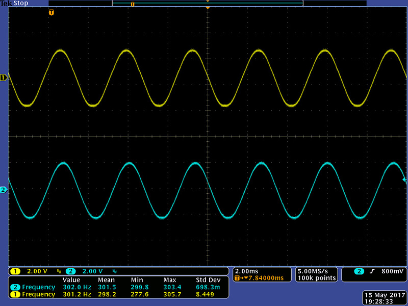
The sine waves are very clean on this oscillator.
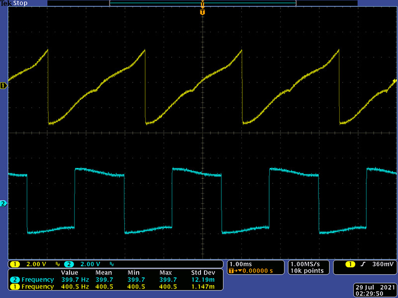
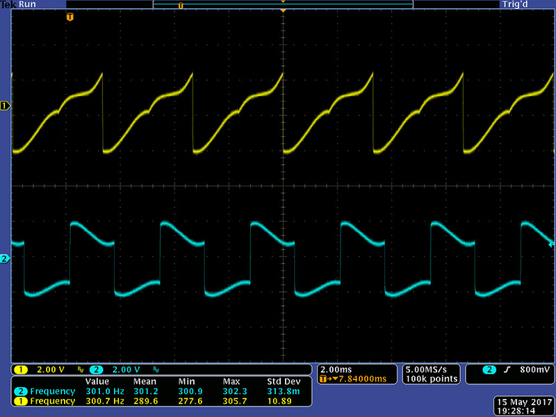
The waveshapping is different between oscillators, one having a waveshape to a saw and the other to a square.
Calibration
Calibration is pretty straightforward on this module although the expo pairs are heated so you need to calibrate that first. Here is the calibration for the heater that I chose.
|
Temperature Adjustment
|
I had to increase R6 and R68 from 91K to 100K to be able to calibrate to 1.2V/Oct. The 1.2V calibration is through the second CV input and attenuator, and potentiometers will have some variation as to their minimum resistance. I set linearity to center, then calibrated at 1.2V for a full octave, then set the CV to 3.6V and adjusted the linearity for a full 3 octaves. Checking at 1.2V and 2.4V the frequencies were correct. Then I set the Frequency to CW, Fine to center, and adjusted the initial trimmer for 5 Hz.
I am not a fan of vintage parts. In most cases there isn't a good reason to use them and most are not in the signal path. J201s are hard to find and some have really poor performance. One of the more counterfeited parts I run across in my repairs are dual PNP pairs. A pair of cut-tape 2N3906s work reasonably well for matched PNP pairs. You can epoxy them together to keep them at the same temperature. I have started using SMT adapter PCBs in some of my builds and repairs.
These are J201 SMT adapters. Not all SOT-23 adapters map the pins to the correct order to replace thru-hole parts. Adapters from PedalPCB and DIYGuitarPedals (shown) do have the correct pinout for J201s on this V3 PCB.
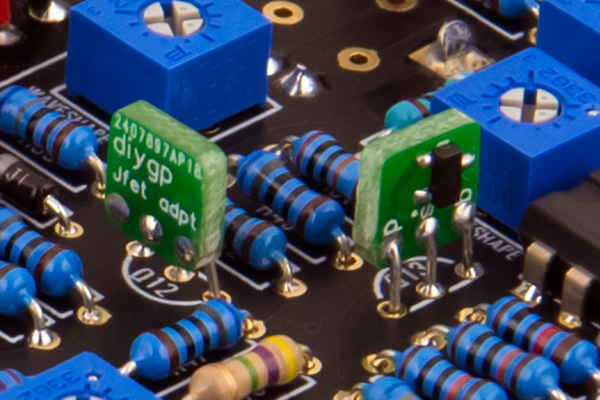
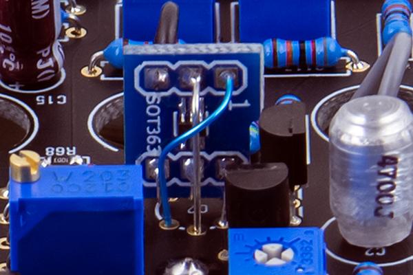
I used Artekit Labs SOT363 SMT adapters with a BC857 SMT for the dual PNP pair. The pinout does not match the PCB so it requires some careful lead forming and a wire on both sides on this V3 PCB.
Other Versions
I did a repair for a customer who had an unknown PCB that closely matched the original design that was built incorrectly. I got it working and then let him do the final tweaking for CV range and scale. Here's his reply. Wow, 7 octaves!
"Many thanks - it reached me yesterday! I proceeded to fit the board back to the panel and implemented several of your suggestions; for the 100K resistors by the freq pot wiper, I changed to 110-111K and this tamed the top end down to 20kHz. Left as-is, it tracked about 4 octaves reasonably. This morning I added 1M trimmers to the HF trim resistor positions, and measuring about 690-700K, and some back and forth adjustment with it and the v/Oct trimmer, after leaving the module powered up for a while, I can now achieve 7 octaves of pretty excellent tracking! I just never expected this would be possible on a 258 - thanks Dave!!!"