 |
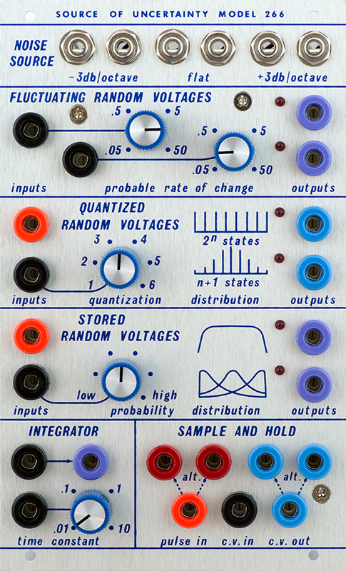
266 Source Of Uncertainty Module |
|
I built a 266 Source Of Uncertainty module for someone else. They sent me a complete kit of parts and I assembled and tested the module. Many of the components are sourced through Mouser but specialized parts, panel, knobs, and PCBs have specific sourcing requirements. I documented all of the 266 functions on my 5U Source of Uncertainty page and extracted a single page description of the 266 from the Allan Strange Electronic Music Systems Techniques and Controls book.
266 description - Electronic Music Systems Techniques and Controls
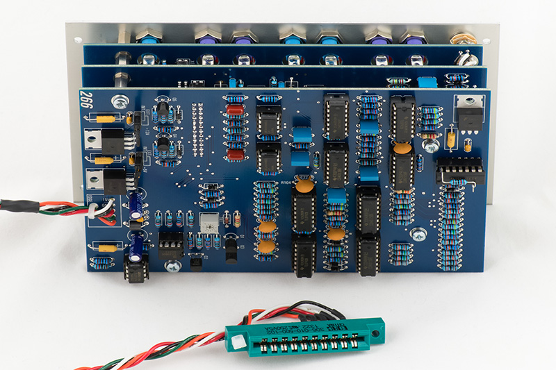
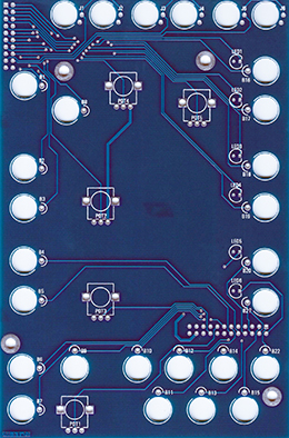
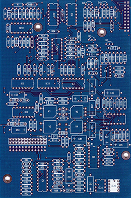
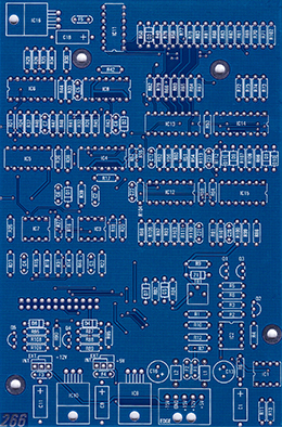
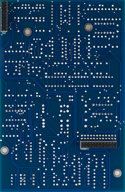
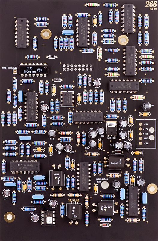
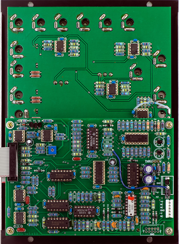
I made reference designators from the PCB images. The components cover the silk screen legends once populated which makes it hard to debug if anything is wrong. Of course the sandwich construction makes it nearly impossible to debug PCB2 anyways.
Construction
There are two build threads and only one modification for the V2 PCB.
266 V2 Source Of Uncertainty modifications
My Modifications
|
Build time for PCB1 and the panel was 2.25 hours. The LEDs do not have a flatted side so the long lead fits on the round side of the silk screen. I insert them fully into the PCB unsoldered. After the panel is mounted you can push them flush with the front panel and solder them in place. I also use color coordinated wire for the banana jacks.
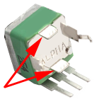
The tabs on the 9mm Alpha potentiometers contact the PCB so I cut the top and bottom tabs off since there are runs directly beneath the tabs. I do not like relying on solder mask for insulation.
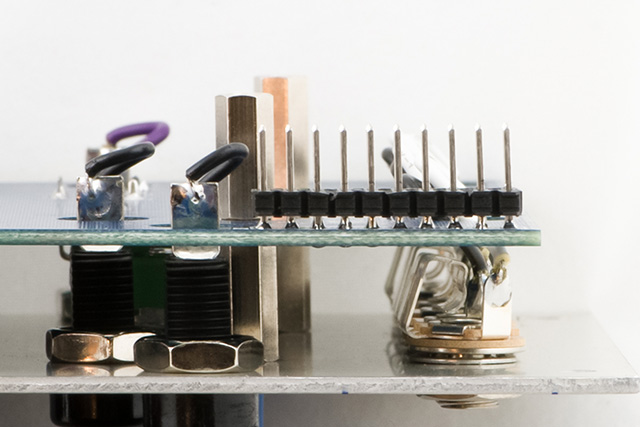
The square pins do not fully seat into the headers with the height of the standoffs. I insert the square pins fully into the female header and assemble the PCBs together. The pins are flush with the PCB and fully inserted into the header so the alignment is correct in all directions and then soldered in place.
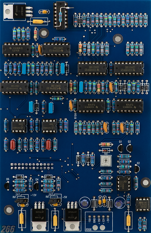
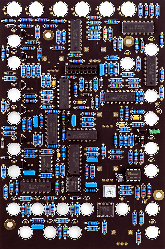
Build time for PCB2 was 4 hours. The resistors take a long time to install since there are so many of them and they are spread all over the PCB. I use Kester .020" diameter #24-6337-6401 331 water soluble core solder so take time every so often to wash the PCB. The potentiometers and vactrols are then added after washing and the wire connections are soldered.

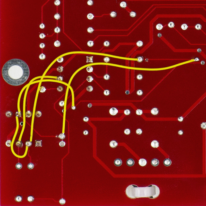
You can see the modification of the cut run and added wire at pin 3 of IC2B in the bottom left corner.
Build time for PCB3 and the power cable was 4 hours. Note that the ferrite beads and the 3 pin jumpers are not on the BOM. I also used 22 µF capacitors instead of 100 µF for C13 and C16. IC11 at the top has the SRV clock modification. I did not clip the IC pin so the modification could easily be reversed.
I chose to mount the female headers on the rear of the PCBs and the square pins on the front of PCB2. That provides better protection for the pins against handling damage.
Operation
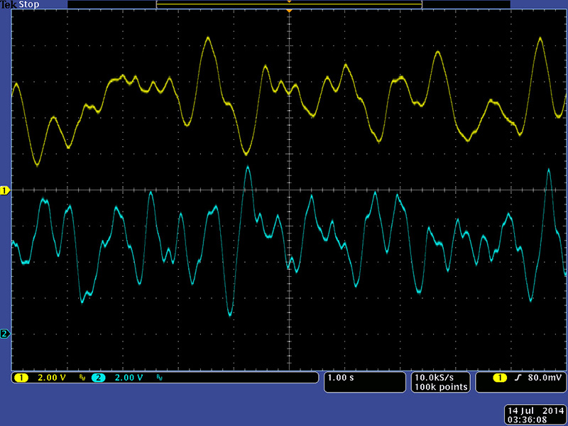
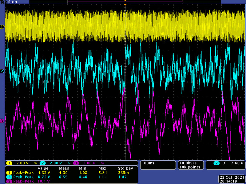
I have more and better scope images along with complete functional descriptions on my 5U 266 Source of Uncertainty page. These scope images are from my verification of this module. These are the three noise outputs.
These are the Fluctuating Random Voltages outputs
These are the Quantized Random Voltages outputs with low states.
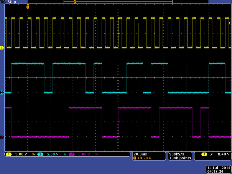
These are the Quantized Random Voltages outputs with high states.
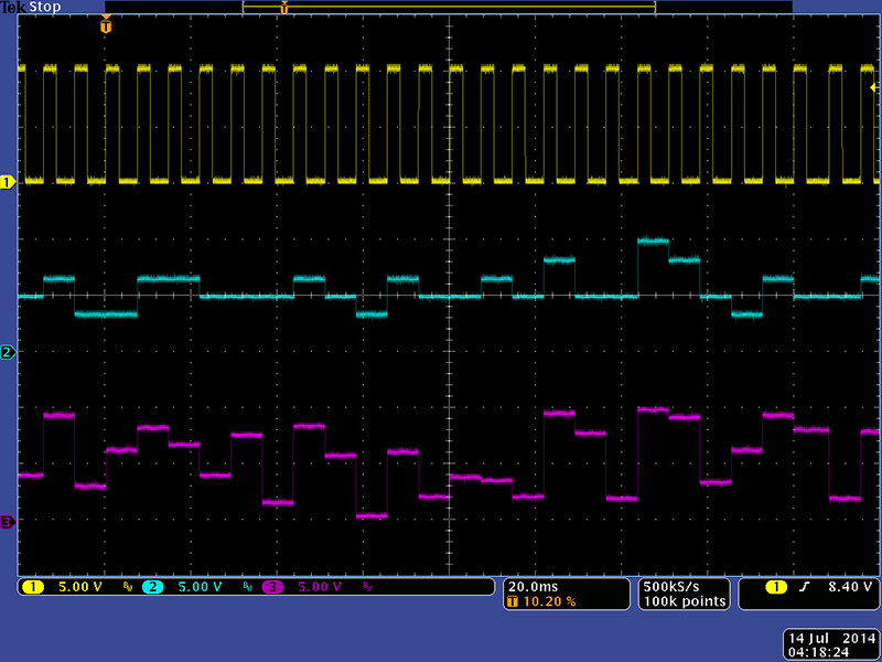
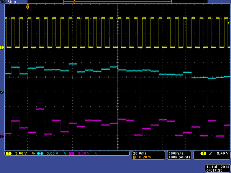
These are the Stored Random Voltages outputs with low probability. Note that they clock on the rising edge with the modification. With low probability the SRV2 output (cyan) stays closer to 0V.
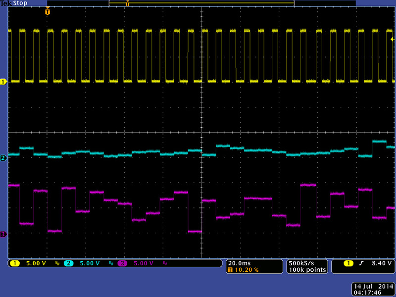
These are the Stored Random Voltages outputs with high probability. With high probability the SRV2 output (cyan) stays closer to 10V.
There is just one trimmer on PCB3. TR1 sets the integration limit of the front panel control and has quite a range. I adjusted TR1 so that the maximum integration time was 10 seconds (1 mV/mS, or 1V/S). This is the integrator output.
These are the S&H alternate clock outputs.
These are the two S&H outputs. You can see them sample on alternate clock edges.

Note that the S&H is really a track and hold. With a higher duty cycle pulse you can see the outputs track the inputs when the pulse is high.
![]()
V2+ (red) PCB
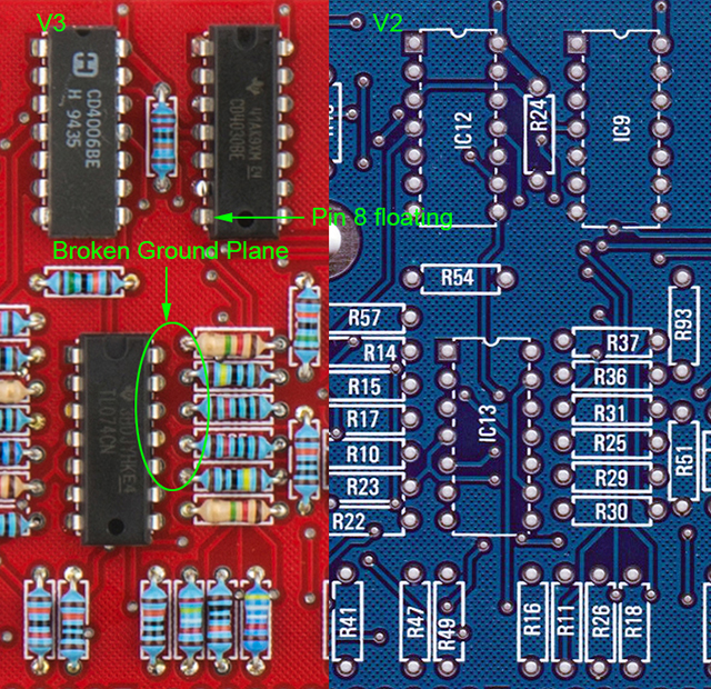
The red PCBs are labeled V3 but Roman refers to the 2 PCB set as V3 so I will call this V2+ since it is a minor cleanup of V2. There is a layout issue on V2+ PCB2 which requires a wire mod. The plane that connects to IC9 pin 7 is isolated and needs to be connected to the ground plane. The CD4030 IC9 has no ground reference and the clock output references to the FRV voltages as can be seen in this scope image. Needless to say QRV stalls for long periods of time but does continue to operate.
The broken ground plane can be seen in this side by side comparison between a V2+ PCB and the V2. Simply run a wire from pin 7 of IC9 to pin 7 of IC12.
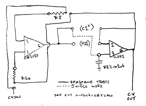
Integrator Modifications
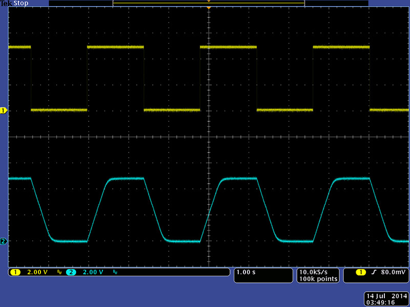
I get a number of questions on my integrator modification. My explanation is on my 5U build with the link in the first paragraph but I don't think most people see it so let me repeat it here. The integration op-amp does not have a DC reference for the negative input. This means the output DC level can drift. This image shows a slew much slower than the input frequency so the amplitude is low but notice the DC offset. The input is a 50% duty cycle square wave so the triangle integration should be centered at 0V.
Adding a 10M resistor across the integration capacitor now provides a DC path for the input and the output is now centered correctly at 0V.
The downside is this 10M resistor now makes the capacitor "leaky" so instead of a linear integration it now has an RC curve as can be seen in this photo.

It has been a long time so I don't remember if I tried higher value resistors. I doubt that the 10 second RC time constant is of much concern to most users, but I decided it would be easy to change the topology to a true linear which is what these modifications do. I would suggest most users simply add a 10M resistor across the integration capacitor.
V2+ Modifications
I built my own 266 V2+ and these are the modifications I chose to do.
266 V2+ Source Of Uncertainty modifications PCB1:
PCB2:
PCB3:
|
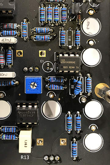
266 V2+ Integrator modifications schematic
These are the modifications for the integrator. You cannot see the front cut on the bottom pad of R8.
V3
V3 is the two PCB..
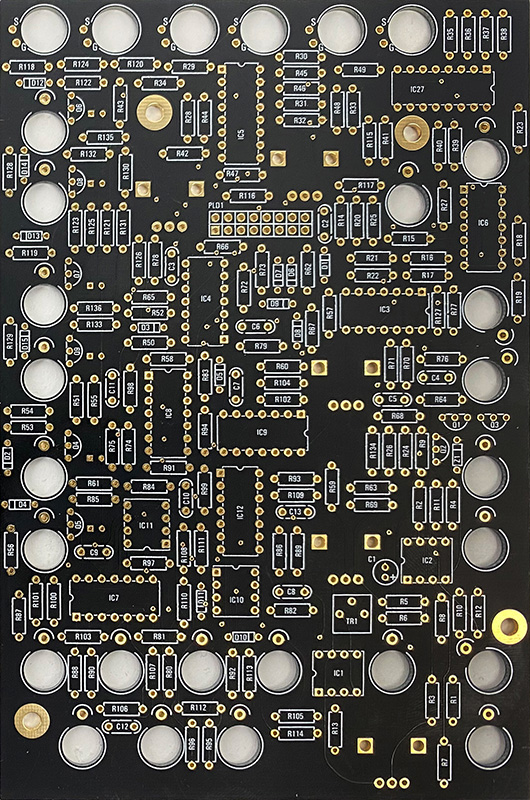
I made a reference diagram from the PCB image.
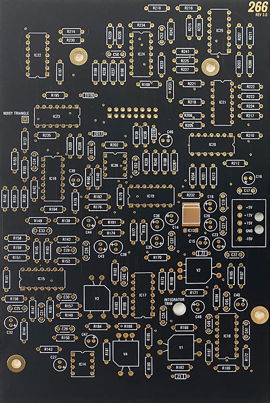
I made a reference diagram from the PCB image.
These two PCBs took just under 8 hours to build. I use SMT J201s with adapters as can be seen on this PCB.
You can still reduce the width of the S&H pulse and modify the integrator. I helped an individual by email and photos come up with these modifications. Since I have never made these on a V3 PCB consider them unverified.
266 V3 Source Of Uncertainty modifications unverified PCB1:
|
266 V3 Integrator modifications schematic
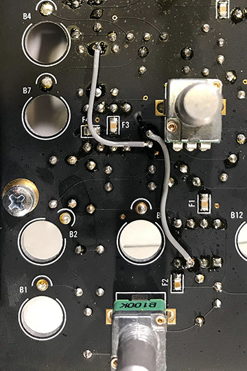
A sharp-eyed reader noticed that R8 and R10 are next to each other and so can be crossed in such a way that no traces need to be cut. Here are his photos.
Epilog
I later received a two board 266 V3 for repairs. One of the issues was the flat and -3dB noise outputs sounded like there were intermittent "breaks" in the signal. The filters for the three outputs are the same as the original and on a scope I could see DC shift on the -3 dB output. The flat output is a separate filter which sums the +3 dB and - 3dB outputs. The -3 dB filter has AC coupling and feedback so the output can shift. I added a 220K resistor across C30 on PCB2 to provide DC feedback which minimized the "breaks".
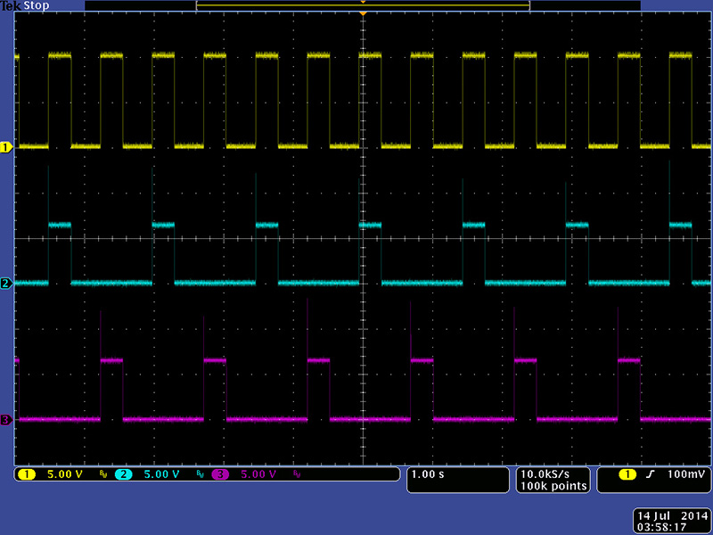
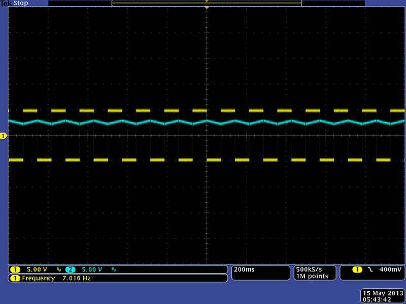
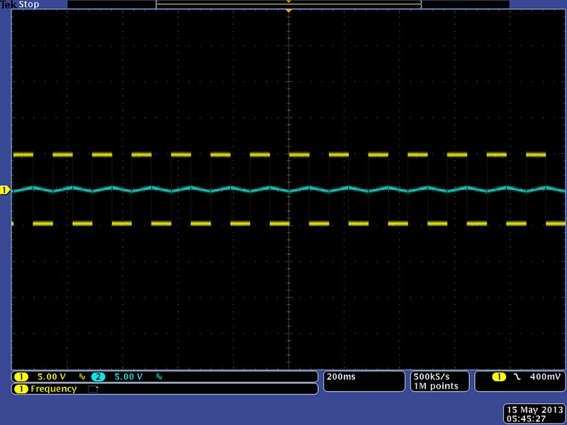
There is a report on the Muffwiggler thread 266 PCB rev 3 fault - QRV outputs swapped that the QRV outputs 2N and N+1 outputs are swapped. He came up with a simple mod that swaps the feedback and outputs for the two op-amps. It is simple enough to check. For N=1 at full CCW both 2N and N+1 = 2 so both outputs just go 0 to 10V as shown in this image.
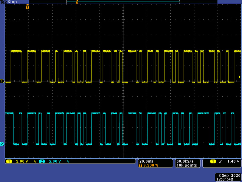
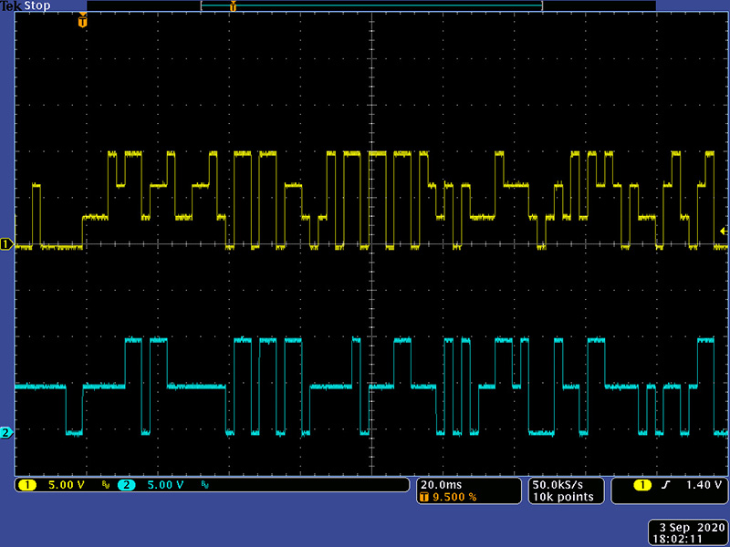
As you turn the control slightly for N=2 then 2N =4 and N+1 = 3. You can see the four states in the yellow trace and the three states in the cyan trace.
Epilog 2
Mike Peake contacted me about a 266 where the FRV would not reliably clock the SRV. After a short time, the SRV would "freeze". I tried to duplicate this on my V2 266 and sure enough it froze. I've never liked how Don drives 10V CMOS from +/-15V op-amps with just resistors. He relies on the internal structure of the CMOS part to clamp the voltage and the resistors limit the current. I theorized that with the FRV, where the output can be above the threshold voltage of the SRV comparator for a longer amount of time, the CMOS logic input might crowbar. I made these changes to the V3 2-board set. I use Schottky diodes for my voltage clamps since I like the lower voltage they provide.
Panel PCB
Change
R19 from 33K to 47K. This is optional but whenever the pulse is high you are
sinking current through the clamp diode so it’s just a waste of power.
Change R18 from a 120K to a diode. The cathode of the diode connects to +10V so
measure continuity to determine which pad.
Add a diode on IC6 between pins 5 and 7 with the anode to pin 7.
Rear PCB
Change
R230 from 10K to 47K. Optional for the same reason. Note on Don’s schematics
it is 100K.
Change R214 from a 120K to a diode. The cathode of the diode connects to +10V so
measure continuity to determine which pad.
Add a diode on IC22 between pins 6 and 7 with the anode to pin 7.
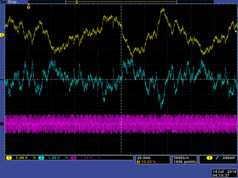
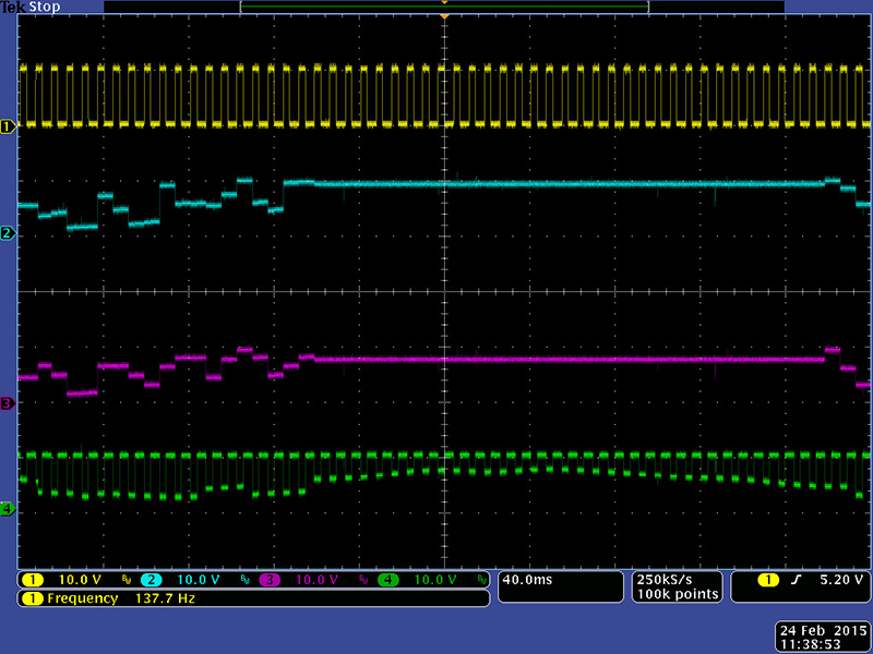
The SRV now runs quite reliably being clocked from the FRV. This scope image is the FRV, the clock pulse to the CMOS gate, and the two SRV outputs. Note the cyan clock is now nicely within the CMOS voltage limits.

West Coast Random Source 5U 266
I was sent a WCRS 266 for modifications and repairs. They wanted CLB_300_RTP lenses installed, the LEDs dimmed, and the noise chip replaced with the Electric Druid. I had to drill out the LED holes to 0.25". Then lenses don't fit tight on a thin panel so I add a 0.25" ID rubber grommet on the inside which holds them flush. I had to shorten each of the LEDs to fit into the lens. The look quite nice. The jacks had been previously replaced and I added Switchcraft washers to match other Dotcom modules. They just slightly obscure "Pulse" on the left.
The two daughter board PCBs were wired together which made it a bit difficult to handle so I didn't take any photos of the middle board with the noise mod. I cut the ground traces away from pin 1 so I could add the Electric Druid noise chip with only lifting pin 2. Pins 5-8 are not connected. The chip needs +5V which is not used on this module, but the Dotcom power connector has it so I added a 10 µF capacitor at the header and flew a wire to pin 1. I added a 0.1 µF capacitor on the rear to pin 8 and wired pin 8 to pin 2 which is ground. I replaced the 39K series resistor with 10K which increases the noise level slightly from the original.
There are 6 individual transistors for the LED drivers which have a 100R resistor from the emitter to ground. I replaced these with 220R to dim the LEDs.
When I verified this module after repairs the QRV Quantization knob was non-functional and the QRV CV jack didn't have much effect. These CV inputs were changed to +/-5V and the QRV CV jack was not normalled so set the control to mid-position. I added a 200K resistor from -15V to the NC pin on the QRV CV jack to restore operation of the Quantization control. The SRV CV jack did not require normalization.
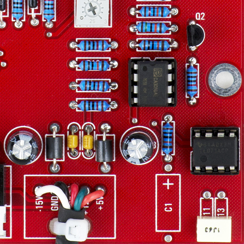
The SRV outputs, however, looked awful. There was a 100 mV deviation on the falling edge of the pulse and the waveforms had a slight tilt to them as if AC coupled. The +10V source is an op-amp as per the original but couldn't hold the voltage stable so it varied several hundred millivolts with the pulse input and SRV states. I modified the regulator op-amp to be a buffer with 0V input by removing three resistors and adding a jumper. I added a 78L10 and capacitor utilizing the MOTM power connector pads. The large blue wire is the new +10V and the small blue wire is the op-amp modification. You can also see the 200K normalization resistor on the motherboard.
The waveforms are all clean now, the LEDs are not blindingly bright, and the Quantization knob functions.