 |
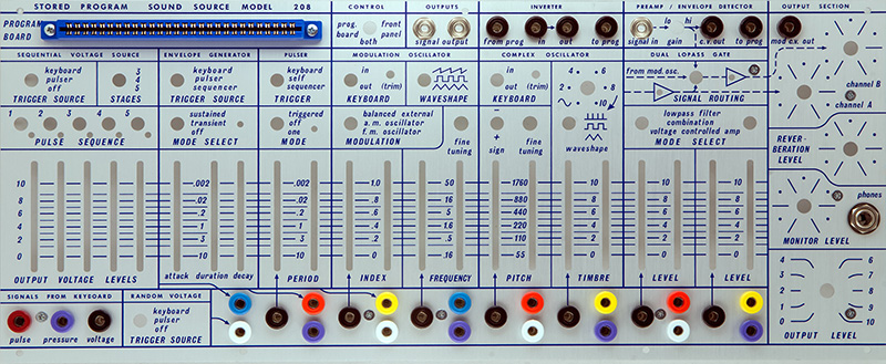
208 V1 Stored
Program |
|
I built this 208 Stored Program Sound Source module for someone else. This is the original two-board set now referred to as V1. They sent me a complete kit of parts and I assembled and tested the module. Many of the components are sourced through Mouser but specialized parts, panel, knobs, and PCBs have specific sourcing requirements.
A scan of the manual |
|
A better color scan of the manual contributed by Luther R. |
Building the PCBs took time since the boards are dense and the reference numbers take time to locate. ICs orientation is not consistent which makes it a bit more error-prone to build but pin 1 is a square pad which makes it easy to verify the correct IC orientation.
The build thread is very long so you have to go through it all to pick up the modifications and build tips. I spent a lot of time studying the PCB assembly to make sure I understood completely how it all went together. 15 mm standoffs are used between the panel and PCB1 and 12 mm standoffs are used between the two PCBs. 2x10 headers connect the two PCBs but the pins are just a bit short for the 12 mm spacing so I soldered the male pins elevated off the PCB (the plastic headers are not seated against the PCB but the pins extend through).
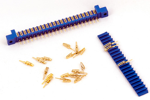
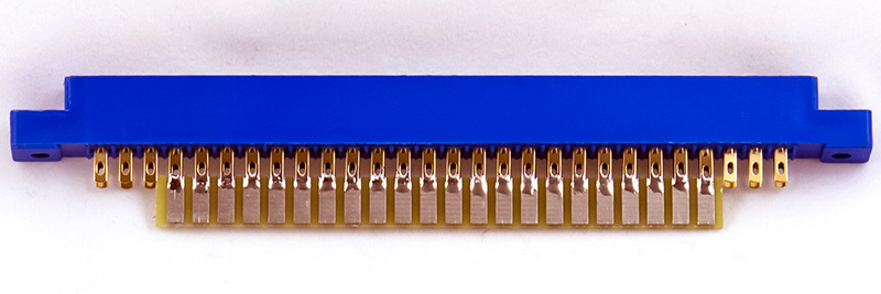
I test fit the 805-44P connector to determine the spacing of the edge fingers but the connector easily splits if it is not soldered into the PCB. DO NOT test fit the edge fingers in this connector without it being soldered in place or you will end up with this! Replacements are available on Amazon and eBay.
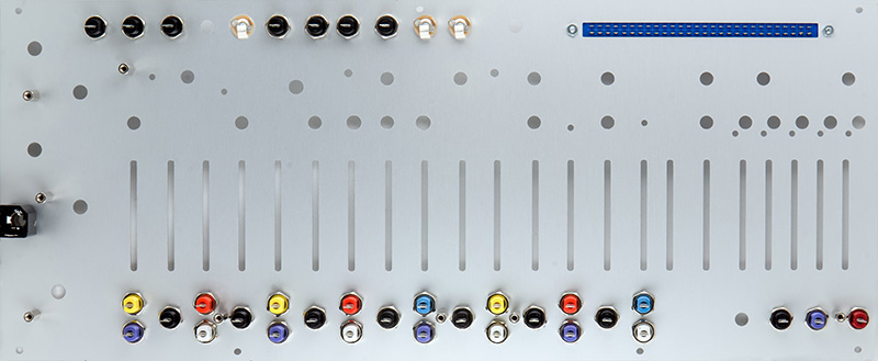
The banana, the three 3.5 mm connectors, and the 1/4" connector install on the panel. There are also eight standoffs that screw to the panel. I soldered the program board connector to the edge finger PCB after the module was assembled.
Here is the process I found best for assembling this module.
|
Assembly Process
|
PCB1 is complete except for the LEDs. Standoffs are installed front and rear to help protect the parts as I work on the PCB.
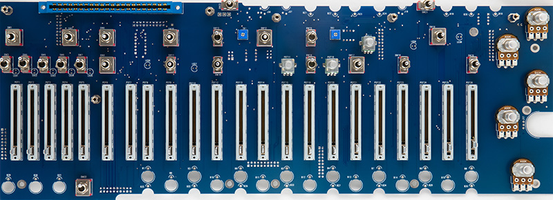
Hi-Res image of PCB1 control side
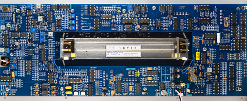
PCB2 is complete except for the reverb tank which I will install last. Standoffs are installed front and rear to help protect the parts as I work on the PCB.
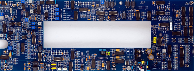
Hi-Res image of PCB2 component side
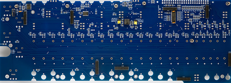
Hi-Res image of PCB1 solder side
The banana, three 3.5 mm jacks, and the 1/4" jacks are now wired to the PCB. I used 1" lengths of colored wire to match the color of the banana jacks. All the correct standoffs are in place for mating PCB2.
Hi-Res image of PCB1 component side and panel wiring
I left a 3.65 mm gap between the top of the edge fingers PCB and the bottom of the Program Board connector. Basically the top of the PCB is even with the bottom of the holes in the terminals. That gives me a reasonable amount of terminal to solder to the finger and a good insertion depth into the 805-44P connector. I cleaned the edge fingers when done with a pink pearl eraser.
This image shows the standoffs in the corners to protect the PCB components and the plastic strips on the male pins above the PCB to allow the pins to fully seat.
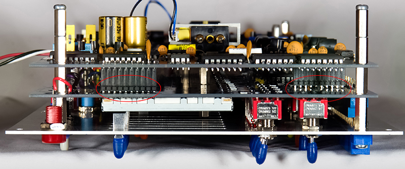
Hi-Res image of module side view
Here is the finished module. It is quite nice looking.
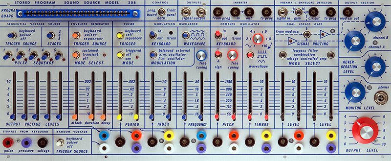
Hi-Res image of 208 Stored Program Sound Source module front
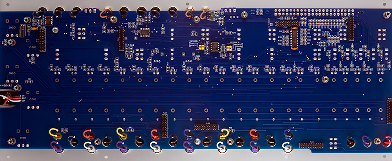
Hi-Res image of 208 Stored Program Sound Source module rear
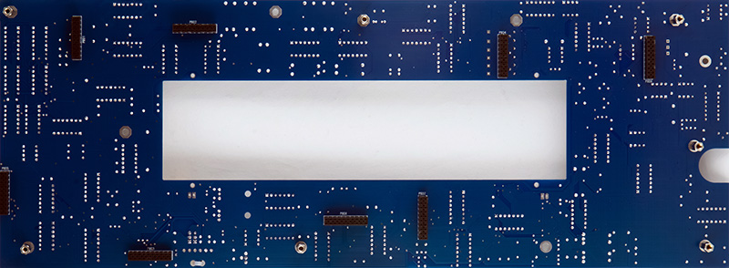
Many of the PCB2 reference numbers are covered by the parts so it is difficult to locate them after the PCB is built. I have a PDF of the reference designators for PCB2.
The Program Connector is NOT compatible with the vintage Buchla or V2 208. The connector on PCB2 is only 44 pins of which 37 are used. I've mapped out the signals as best I can. There is only one signal common between V1 and V2. Several of the CV inputs have dual pins. These pins are not connected but indeed are two separate CV inputs for the same function. In addition, often there is a connection directly to the banana jack. I have labeled these as such.
208 Program Board Connector Pin Definitions (unverified)
I did build a perfBOB expander for a V1 208.
Modifications
Modifications are spread throughout the build thread. I have collected the ones I use here.
Remove IC3 and set all four jumpers to Original on PCB1.
The headphone amplifiers IC45 and IC46 have separate Q and N grounds. If these are not connected on PCB2 by the jumper, these parts can oscillate at high frequency and destroy themselves. Add a 0.1 µF ceramic capacitor on the rear between pins 14 and 7 on IC45 and IC46 on PCB2.
Change R233 from 390K to 1M on PCB2.
Change R193 from 10K to 1K on PCB2.
If you cannot trim a good sine shape, change R252 from 10K to 6K8 on PCB2.
If the MO is offset to very low frequencies then increase R233 on PCB1. I used 499K to shift the MO up to 50 Hz per the slider value.
For 1.2V/Oct, change R240 to 80K6 and R55 to 68K on PCB1.
One MO had a large offset that required R233=499K. It also would not calibrate to 1.2V/Oct without leaving R240 as 91K.
Not included in the build threads is R282 and R285 are swapped. This affects the timbre circuit. R282 should be 3k3 and R285 should be 33K.
The headphones are coupled with 470 µF capacitors. These capacitors can retain a charge with no headphone connected and when inserting a plug can result in a loud "pop". Simply put a 10K resistor from each terminal to ground on the headphone jack.
Someone sent me this modification to change the "off" position of the EG to "cycle". It is similar to the cycle circuitry on the 281.
Calibration
Calibration is documented on the EMCloned Build Thread. Thresholds for different functions required a fairly precise 10 volt pulse. I've extracted the calibration instructions into the following PDF file.
Calibration was pretty straightforward except for the 1.2V scaling. Setting the complex oscillator range from 55 Hz to 5 KHz would not allow the front panel trimmer to reach 1.2V/octave. The front panel scale and the range control are two separate gains in the CV circuitry. I adjusted the front panel trimmer to about 3/4 so I would have some margin and then adjusted the range control for a final 1.2V/octave setting. The resulting complex oscillator range was a bit broader which is nice. With the fine tune to full CW the complex oscillator range is quite high although the amplitude drops off past 6.5 KHz.
| Complex Oscillator Range with front panel control | ||
| Min Frequency | Max Frequency | |
|
Fine Tune at full CCW: |
44 Hz | 6.5 KHz |
|
Fine Tune at full CW: |
100 Hz | 18 KHz |
I likewise had similar issues with the modulation oscillator and followed the same procedure for setting the tracking to 1.2V/octave. It likewise had a broad range mostly at the very low frequencies.
| Modulation Oscillator Range with front panel control | ||
| Min Frequency | Max Frequency | |
| Fine Tune at full CCW: | 0.05 Hz | 24 Hz |
|
Fine Tune at full CW: |
0.9 Hz | 41 KHz |
I found that I could shift this range slightly up by adding a small amount of control voltage at the IC30A summer. A 1M resistor from pin 2 to 7 would shift the range up nicely although I left it unmodified.
| Modified Modulation Oscillator Range with front panel control | ||
| Min Frequency | Max Frequency | |
| Fine Tune at full CCW: | 0.1 Hz | 53 KHz |
|
Fine Tune at full CW: |
0.2 Hz | 91 Hz |
Verification
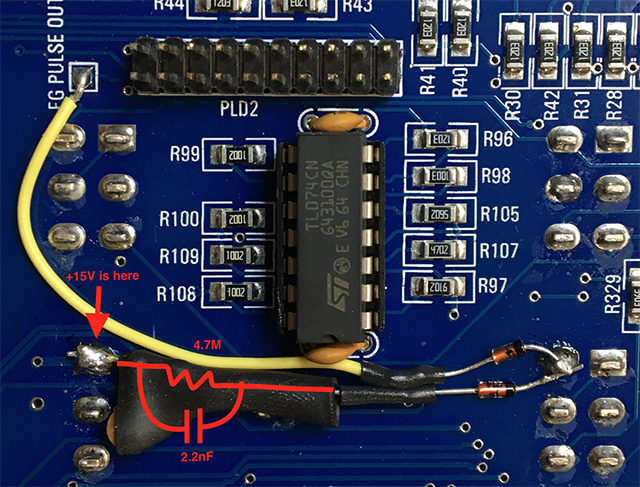
In this scope image you can see a two level keyboard pulse I generated with my ComputerVoltageSource. In transient mode the envelope delay is based on the delay control setting. It actually is delayed by the trigger portion of the keyboard pulse and then by the delay control setting but the trigger is short so it is not noticeable.
![]()
In the sustain position the gain is increased such that the pulse from IC19-10 is the entire width of the keyboard pulse which is longer than the delay control setting and dominates.
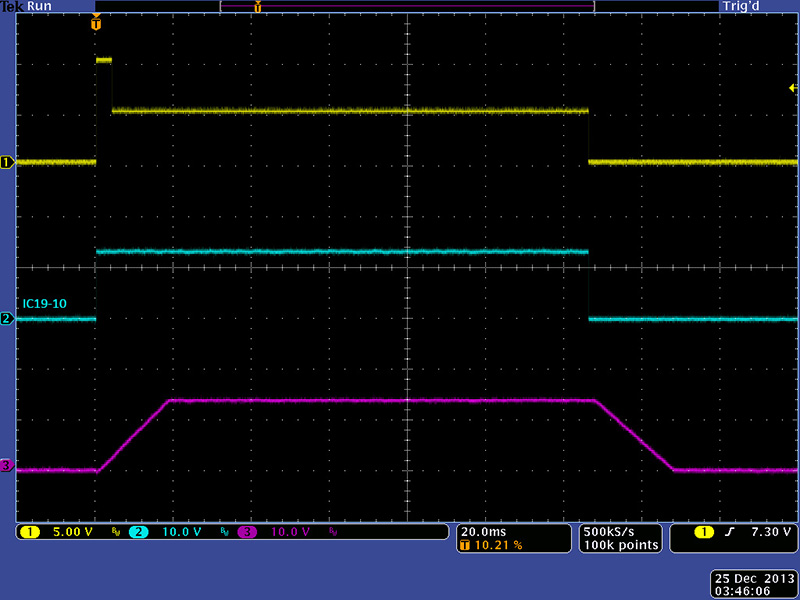
The four random outputs are unique. Output 1 (top is just an attenuated version of output 4 (bottom).
Operation
I have just a short video of the 208 Stored Program Sound Source running a short patch. This is an interesting module.